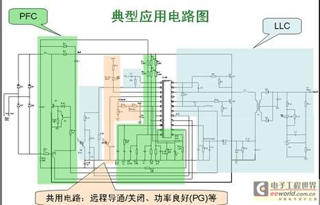
Computers, servers and flat-panel TVs have always been important targets for energy efficiency regulation agencies. These devices must meet the latest energy efficiency requirements while meeting high performance. As a leading manufacturer, ON Semiconductor has been committed to launching power controllers that meet the latest energy efficiency regulations. This article will introduce the main features and application design points of ON Semiconductor's high-efficiency, high-performance power factor correction (PFC) and half-bridge resonant dual inductor plus single capacitor (LLC) combination controller NCP1910 used in computer ATX power supplies and flat-panel TVs, to help engineers better use NCP1910 for related power supply designs.
- Fixed frequency continuous conduction mode (CCM) PFC is available in 65kHz, 100kHz, 133kHz and 200kHz options;
- Programmable overcurrent threshold provides optimized sense resistor;
- Over-power limiting can limit current according to the average input voltage;
- PFC abnormal protection, in the event of a PFC abnormality, the device stops working even if the input is a high line voltage;
- Undervoltage protection prevents damage in case of wrong connections in the feedback network;
-
Fast transient response to maintain V
bulk
regulation:
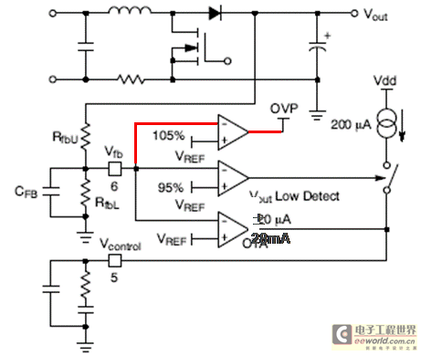
--Overvoltage protection automatically restores the OVP threshold (105% of regulation level);
--Dynamic response enhancer uses its internal 200 µA current source to speed up the regulation loop when V
bulk
drops below 95% of its regulation level;
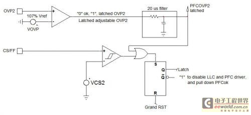
- Redundant OVP (OVP2) uses a dedicated pin to latch V bulk OVP;
- Adjustable line input undervoltage with 50 ms blanking time to avoid damage at low input voltage;
- V in 2 feed-forward optimizes power factor;
- Power Boost can adjust V bulk under extreme line transient conditions (e.g. 264 Vac → 90 Vac);
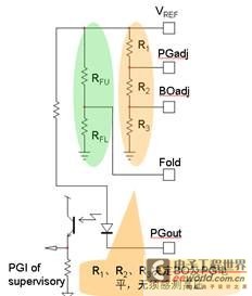
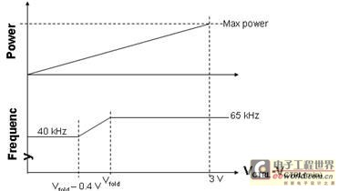
- Adjustable frequency retardation improves light load energy efficiency;
- Soft start;
- The totem pole drive capability is ±1.0 A gate driver.
- Wide operating frequency range from 25 kHz to 500 kHz;
- The fixed dead time on the board is 300 ns to avoid shot-through;
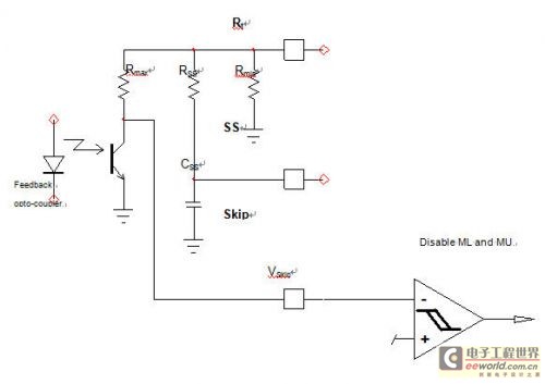
- During soft start or restart, a dedicated pin discharges the SS capacitor to ground, providing a smooth output voltage rise. When LLC is turned off by the CS/FF pin (> 1V) or the BO function, the SS pin discharges C SS and provides a pure soft start.
- High voltage driver gate drive is + 0.5 A -1.0 A;
-
Dual fault protection levels are located at the CS/FF pin:
--CS/FF > 1 V: LLC converter immediately increases switching frequency by grounding CSS . This is an auto-recovery protection mode; --CS/FF > 1.5 V: Latched when a fault is severe and causes CS/FF to be above 1.5 V; - Adjustable input undervoltage (BO), FB pin voltage accounts for a portion of V bulk , no high-voltage sense rail is required, which can save power;
- NCP1910B has a skip cycle working function. When the feedback pin voltage is lower than 0.4 V, the LLC driver enters the skip cycle mode, reducing the frequency and improving the light load energy efficiency.
Previous article:Optocoupler-free flyback DC/DC controller benefits video security
Next article:Solar LED Street Light Solution Using STM32 MCU
- Popular Resources
- Popular amplifiers
- MathWorks and NXP Collaborate to Launch Model-Based Design Toolbox for Battery Management Systems
- STMicroelectronics' advanced galvanically isolated gate driver STGAP3S provides flexible protection for IGBTs and SiC MOSFETs
- New diaphragm-free solid-state lithium battery technology is launched: the distance between the positive and negative electrodes is less than 0.000001 meters
- [“Source” Observe the Autumn Series] Application and testing of the next generation of semiconductor gallium oxide device photodetectors
- 采用自主设计封装,绝缘电阻显著提高!ROHM开发出更高电压xEV系统的SiC肖特基势垒二极管
- Will GaN replace SiC? PI's disruptive 1700V InnoMux2 is here to demonstrate
- From Isolation to the Third and a Half Generation: Understanding Naxinwei's Gate Driver IC in One Article
- The appeal of 48 V technology: importance, benefits and key factors in system-level applications
- Important breakthrough in recycling of used lithium-ion batteries
- Innolux's intelligent steer-by-wire solution makes cars smarter and safer
- 8051 MCU - Parity Check
- How to efficiently balance the sensitivity of tactile sensing interfaces
- What should I do if the servo motor shakes? What causes the servo motor to shake quickly?
- 【Brushless Motor】Analysis of three-phase BLDC motor and sharing of two popular development boards
- Midea Industrial Technology's subsidiaries Clou Electronics and Hekang New Energy jointly appeared at the Munich Battery Energy Storage Exhibition and Solar Energy Exhibition
- Guoxin Sichen | Application of ferroelectric memory PB85RS2MC in power battery management, with a capacity of 2M
- Analysis of common faults of frequency converter
- In a head-on competition with Qualcomm, what kind of cockpit products has Intel come up with?
- Dalian Rongke's all-vanadium liquid flow battery energy storage equipment industrialization project has entered the sprint stage before production
- Allegro MicroSystems Introduces Advanced Magnetic and Inductive Position Sensing Solutions at Electronica 2024
- Car key in the left hand, liveness detection radar in the right hand, UWB is imperative for cars!
- After a decade of rapid development, domestic CIS has entered the market
- Aegis Dagger Battery + Thor EM-i Super Hybrid, Geely New Energy has thrown out two "king bombs"
- A brief discussion on functional safety - fault, error, and failure
- In the smart car 2.0 cycle, these core industry chains are facing major opportunities!
- The United States and Japan are developing new batteries. CATL faces challenges? How should China's new energy battery industry respond?
- Murata launches high-precision 6-axis inertial sensor for automobiles
- Ford patents pre-charge alarm to help save costs and respond to emergencies
- New real-time microcontroller system from Texas Instruments enables smarter processing in automotive and industrial applications
- I need help from all the experts regarding the SPI communication between STM32 master and slave. Thanks in advance!
- Can WIFI6 increase Internet speed?
- This hand-rubbing IoT smart home system is amazing
- Use several practical cases to analyze how to solve electromagnetic compatibility (ESD) problems
- EETalk| Which indicator do you pay most attention to when buying a power supply?
- Super low price | Try cheap and easy-to-use power chips, MPS Thanksgiving and feedback season!
- Stumped by ESP32 Arduino
- 【Xingkong board Python programming learning main control board】4. Xingkong board opencv test
- In the RF field, 90nm GaN has a promising future
- The World Cup ended 6-2 yesterday. Did you watch the game?







 FPGA Principle and Structure (Zhao Qian)


 京公网安备 11010802033920号