introduction
In low-voltage and high-current applications, push-pull circuits are widely used due to their simple structure and high core utilization. However, the traditional push-pull circuit has the following shortcomings:
1) Due to the existence of primary leakage inductance, when the power tube is turned off, a large voltage spike occurs at the drain-source electrode;
2) The ampere-second integral of the input current ripple is large, so the volume of the input filter is large.
This article adds a clamping capacitor on the basis of the traditional push-pull circuit, which can solve the two shortcomings of the traditional circuit mentioned above.
1 Working principle of push-pull forward circuit

1 Working principle of push-pull forward circuit
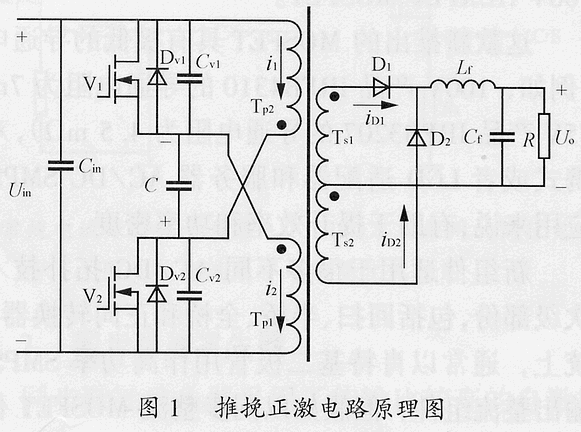
As shown in Figure 1, the two main power switching tubes V1 and V2 of the converter and the two primary windings Tp1 and Tp2 with Np turns are alternately connected to form a loop, and a loop is connected between the two midpoints of the loop. Clamping capacitor C. Cin is the input capacitance, Dv1 and Dv2 are the parasitic anti-parallel diodes of the two main power switch tubes. D1 and D2 form a double half-wave rectifier circuit.
The positive pole of the power supply→Tp2→C→Tp1→the negative pole of the power supply forms a loop. Ignoring the leakage inductance of the transformer, the sum of the voltages applied to the two windings on the primary side of the transformer is zero. The voltage on C is Uin, which is positive below and negative above. The other circuit is the positive pole of the power supply→V1→C→V2→the negative pole of the power supply. According to Kirchhoff's circuit law, we can get
Uds1+Uds2=Uin+Uc=2Uin
Therefore, when a certain switch tube is turned on, the voltage of the other switch tube is clamped at 2Uin; when both switch tubes are turned off, the voltage of each switch tube is Uin. Before analyzing the working mode of the push-pull forward circuit, make the following settings:

1) V1, V2, D1, and D2 are all ideal devices, and the conduction voltage drop is negligible;
2) C is larger, and the voltage at both ends remains basically unchanged Uin during the working process;
3) The filter inductor Lf is large and can be regarded as a constant current source in a short period of time, and the current remains unchanged; the output current Io=Uo/R in steady state;
4) The number of turns of the primary winding is Np, the excitation inductance and leakage inductance are both Lm and Lσ, the number of secondary turns is Ns, and the turns ratio n=Ns/Np;
5) The switching period Ts, the turn-on time of each cycle of V1 and V2 is ton, and the duty cycle of V1 and V2 is D=ton/Ts;
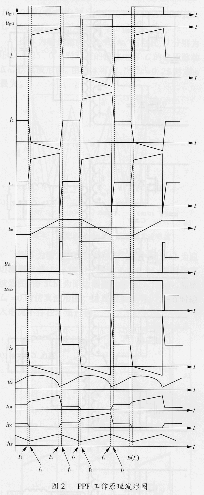
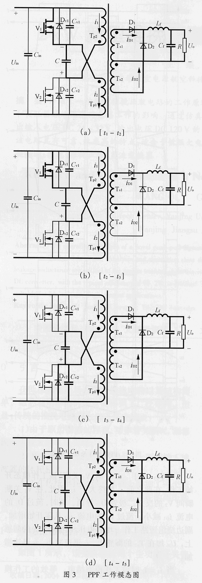
Figure 2 is a waveform diagram of the working principle of the push-pull forward circuit, which is divided into 8 working modes. 1) [t1-t2] Before t1, both V1 and V2 are turned off, and the input current circulates along the positive pole of the power supply→Tp2→C→Tp1→the negative pole of the power supply loop. The circulating current is Ia=nDIo[1] (detailed analysis is in Chapter 1) given in Section 2). The voltage of the primary and secondary windings is 0, and D1 and D2 are turned on at the same time. When V1 is turned on at time t1, Uin is added to the leakage inductance of Tp1, i1 increases rapidly; Uc is added to the leakage inductance of Tp2, i2 decreases rapidly and increases in the opposite direction. Correspondingly, the current iD1 flowing through D1 on the secondary side increases, and the current iD2 flowing through D2 decreases. At time t2, D2 ends at iD2=0. The equivalent circuit diagram of this mode is shown in Figure 3(a), and the duration is


In the formula: iLfmin is the filter inductor current at time t1.
2) [t2-t3] When D2 is cut off, this working mode starts to work. Uin is added to the excitation inductance and leakage inductance of Tp1, and Uc is added to the excitation inductance and leakage inductance of Tp2, each bearing the excitation current and load current. Half of the change rate, at this time the primary is equivalent to two single-ended forward circuits working in parallel [2][3][4]. i1 increases and i2 increases inversely. The working mode is shown in Figure 3(b), and the duration is

3) [t3-t4] At t3 moment, V1 is turned off, and this working mode starts to work. Before this, i1 is always greater than i2. Therefore, the anti-parallel diode Dv2 of V2 turns on at the moment when V1 turns off. At the same time, the current iD1 flowing through D1 decreases, the current iD2 flowing through D2 increases from zero, and the secondary winding works in a short circuit. The capacitor voltage Uc is added to the leakage inductance of Tp1, and Uin is added to the leakage inductance of Tp2. i1 decreases rapidly and i2 increases rapidly.
The working mode ends when i1=i2. The equivalent working mode circuit is shown in Figure 3(c), and the duration is

In the formula: iLfmax is the filter inductor current at time t3.
4) [t4-t5] During this period, both V1 and V2 are turned off. The average leakage inductance current (circulation current) Ia flows through the positive electrode of the power supply→Tp2→C→Tp1→the negative electrode loop of the power supply. Since the power supply voltage and the clamping capacitor voltage are equal, the voltages applied to the two primary windings are both zero, and the circulating current Ia remains unchanged. The equivalent working mode is shown in Figure 3(d), with a duration of


5) [t5-t9] At time t5, V2 is turned on to start the work of the second half cycle. The working mode is the same as the first half cycle, except that the direction of the excitation current is opposite, completing the demagnetization of the transformer.
2 Circulation analysis

2 Circulation analysis
Assuming that the power loss of the push-pull forward converter is zero, according to the law of conservation of energy in the system, the power input power in the half cycle Ts/2 is

In order to simplify the analysis of the problem, we assume that the following ideal conditions hold:
1) The commutation of the two windings on the primary side is completed instantly, that is
Δt1-2=0, Δt3-4=0;
2) The excitation inductor Lm and the filter inductor Lf are large, the excitation current is zero, and Lf can be regarded as a constant current source, and it is obtained
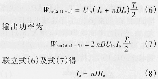

It can be seen that when the working duty cycle D of the circuit is large, the primary side circulation time is short and the circulation flow value is large; as the output power increases, the circulation current value also increases.
3 Analysis of the influence of main parameters on circuit operation
3.1 The role and selection of clamping capacitor C
3.1.1 Two main functions of clamping capacitors
1) Suppress the switch tube turn-off voltage spike. As shown in Figure 1, when V1 is turned off, C provides a low-impedance energy release circuit of Dv2→C→Tp1 to the primary leakage inductance of the transformer. Clamping the drain-source voltage of V1 at Uin+Uc effectively suppresses the voltage spike of the switching tube. The clamping capacitor C stores electrical energy when the switch is fully turned off and releases the energy to the load when it is turned on. Theoretically, there is no energy loss.
2) Reduce the volume of the input filter. Compared with the traditional push-pull circuit, the clamping capacitor in the push-pull forward circuit provides a freewheeling circuit during the turn-off period of the switch tube. It is precisely because of the existence of the freewheeling loop that the ampere-second integral of the input current ripple of the push-pull forward circuit is smaller than that of other topologies. Therefore, the size of the input filter can be reduced.

2) Reduce the volume of the input filter. Compared with the traditional push-pull circuit, the clamping capacitor in the push-pull forward circuit provides a freewheeling circuit during the turn-off period of the switch tube. It is precisely because of the existence of the freewheeling loop that the ampere-second integral of the input current ripple of the push-pull forward circuit is smaller than that of other topologies. Therefore, the size of the input filter can be reduced.
3.1.2 Selection of clamping capacitor
According to the previous analysis, the voltage ripple Δuc of the clamping capacitor C is determined by the amount of charge during the circulating current, that is

The circuit working cycle Ts, the maximum load current Io, and the transformer turns ratio n have been determined before design. In engineering practice, Δuc=20% Uin is selected. Therefore, the required capacitance value can be calculated based on the working range of the duty cycle D. At the same time, in order to reduce the impact of capacitor ESR, a parallel connection of multiple film capacitors is generally adopted.
3.2 Impact of transformer leakage inductance on PPF operation
For an ideal transformer, the leakage inductance Lσ of the transformer is 0. When whichever power tube is turned off, the transformer winding current is instantly reduced to 0, and there is no circulating current during the period when both switching tubes are turned off. In fact, leakage inductance exists in any transformer. In the push-pull forward circuit, when both switching tubes are turned off, the energy of the primary leakage inductance charges C through the positive electrode of Uin→Tp2→C→Tp1→Uin negative electrode loop. Circulating current creates voltage ripples on the clamping capacitor. At the same time, reducing the leakage inductance of the primary side can reduce the commutation time when the power tube is turned on, that is, reducing the loss of duty cycle, thereby improving the utilization of the transformer and reducing the loss of circuit operation.
From the above analysis, it can be seen that reducing leakage inductance can improve the efficiency of the system. Therefore, transformers often use the method of winding between the primary and secondary sides to reduce the value of leakage inductance.
4 Simulation and Experiment

4 Simulation and Experiment
4.1 Simulation analysis
Based on the above analysis, a principle simulation of the work of PPF was carried out. The main simulation circuit is shown in Figure 1. The main parameters of the simulation are: Uin=28V, C=70μF, n=6, Io=10A, Lf=160μH, Cf=680μF/400V×2, Ts=20μs.
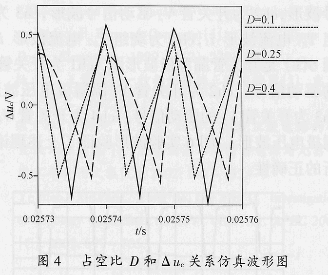
Figure 4 shows the simulation waveform diagram of the voltage pulsation Δuc of the clamping capacitor C when the output current Io=10A and the duty cycle D are 0.1, 0.25 and 0.4 respectively. It can be seen from Figure 4 that Δuc is the largest when D=0.25.
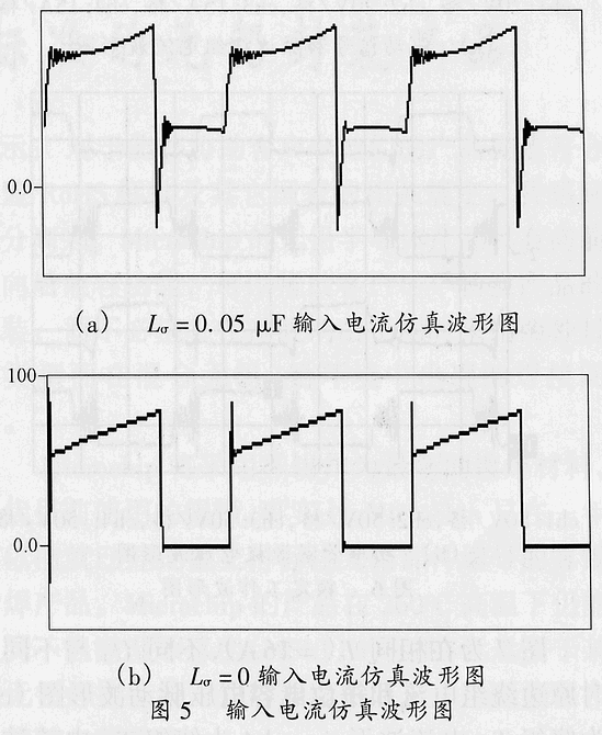
Figure 5 shows the input current simulation waveform. Figure 5(a) shows the simulation waveform when the primary side magnetizing inductance Lm=12μH and the leakage inductance Lσ=0.05μF; Figure 5(b) shows the primary side exciting inductance Lm=12μH and the leakage inductance. Simulation waveform diagram when Lσ=0. The simulation results show that when Lσ=0, there is no circulation process in the input current.
4.2 Experimental results

4.2 Experimental results
According to the relevant technical requirements, a 2kW DC/DC converter with input DC24V~32V and output DC120V was developed. The system parameters are: switching frequency fs=50kHz; main power switch tube is IXTK180N15; rectifier diode is DSEP60-06A; clamp capacitor C=70μF; filter inductor Lf=160μH; filter capacitor Cf=680μF/400V×2; main transformer turns Ratio n=6, the magnetic core is EE55×2.
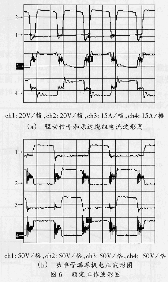
Figure 6 is the experimental waveform diagram under rated load, in which Figure 6(a) is the primary winding current waveform diagram (ch1 is the driving signal waveform of the switching tube V1, ch2 is the driving signal waveform of the switching tube V2, ch3 is the current waveform i1 of the winding Tp1, ch4 is the current waveform i2 of winding Tp2); Figure 6(b) is the drain-source waveform diagram of the switching tube (ch1 is the driving signal of the switching tube V1, ch2 is the source-drain voltage waveform of the switching tube V1, ch3 is the driving signal of the switching tube V2 signal, ch4 is the source-drain voltage waveform of switch tube V2). The experimental waveform in Figure 6 verifies the correctness of the above theoretical analysis.
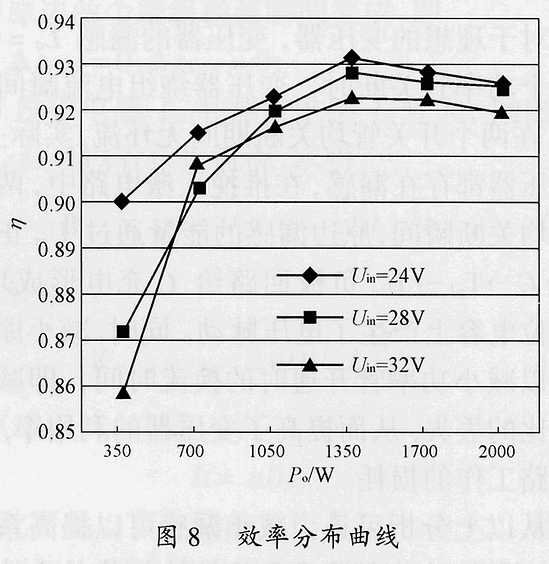
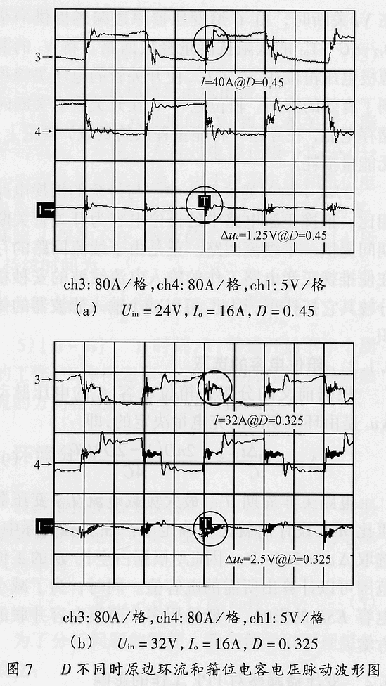
Figure 7 shows the primary winding current and clamping capacitor voltage pulsation waveforms at the same Io (=16A), different Uin and different D (ch3 is the current waveform i1 of winding Tp1, ch4 is the current waveform i2 of winding Tp2, ch1 is the clamp Capacitor voltage pulsation Δuc waveform). The experimental waveform fully demonstrates the correctness of the circulating current analysis in Section 2 and the clamping capacitor selection principle in Section 3.1.2.

Figure 7 shows the primary winding current and clamping capacitor voltage pulsation waveforms at the same Io (=16A), different Uin and different D (ch3 is the current waveform i1 of winding Tp1, ch4 is the current waveform i2 of winding Tp2, ch1 is the clamp Capacitor voltage pulsation Δuc waveform). The experimental waveform fully demonstrates the correctness of the circulating current analysis in Section 2 and the clamping capacitor selection principle in Section 3.1.2.
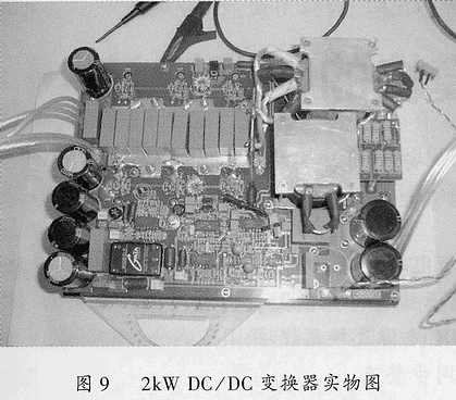
Figure 8 shows the efficiency distribution curve of the 2kW DC/DC converter. The efficiency of the converter can reach 93.2%. Figure 9 is a physical diagram of the converter.
5 Conclusion
The simulation analysis and experimental results verify the correctness of the theoretical analysis and formula derivation, showing that the push-pull forward circuit has the following advantages when applied to this converter:
1) The drain-source voltage spike of the switch tube is suppressed, the voltage stress and power loss of the switch tube are reduced [5], and the overall efficiency of the machine is high;
2) The transformer is bidirectionally magnetized and the magnetic core utilization rate is high;
3) The ampere-second integral of the input current ripple is smaller than that of other topologies, which reduces the volume of the input filter.

3) The ampere-second integral of the input current ripple is smaller than that of other topologies, which reduces the volume of the input filter.
This converter has high engineering practical value especially in low-voltage and high-current applications.
Previous article:Application of low-cost DC/DC converter 34063
Next article:Application of 80C196MH in square wave three-phase brushless DC motor
- Popular Resources
- Popular amplifiers
Recommended Content
Latest Power Management Articles
- MathWorks and NXP Collaborate to Launch Model-Based Design Toolbox for Battery Management Systems
- STMicroelectronics' advanced galvanically isolated gate driver STGAP3S provides flexible protection for IGBTs and SiC MOSFETs
- New diaphragm-free solid-state lithium battery technology is launched: the distance between the positive and negative electrodes is less than 0.000001 meters
- [“Source” Observe the Autumn Series] Application and testing of the next generation of semiconductor gallium oxide device photodetectors
- 采用自主设计封装,绝缘电阻显著提高!ROHM开发出更高电压xEV系统的SiC肖特基势垒二极管
- Will GaN replace SiC? PI's disruptive 1700V InnoMux2 is here to demonstrate
- From Isolation to the Third and a Half Generation: Understanding Naxinwei's Gate Driver IC in One Article
- The appeal of 48 V technology: importance, benefits and key factors in system-level applications
- Important breakthrough in recycling of used lithium-ion batteries
MoreSelected Circuit Diagrams
MorePopular Articles
- Innolux's intelligent steer-by-wire solution makes cars smarter and safer
- 8051 MCU - Parity Check
- How to efficiently balance the sensitivity of tactile sensing interfaces
- What should I do if the servo motor shakes? What causes the servo motor to shake quickly?
- 【Brushless Motor】Analysis of three-phase BLDC motor and sharing of two popular development boards
- Midea Industrial Technology's subsidiaries Clou Electronics and Hekang New Energy jointly appeared at the Munich Battery Energy Storage Exhibition and Solar Energy Exhibition
- Guoxin Sichen | Application of ferroelectric memory PB85RS2MC in power battery management, with a capacity of 2M
- Analysis of common faults of frequency converter
- In a head-on competition with Qualcomm, what kind of cockpit products has Intel come up with?
- Dalian Rongke's all-vanadium liquid flow battery energy storage equipment industrialization project has entered the sprint stage before production
MoreDaily News
- Allegro MicroSystems Introduces Advanced Magnetic and Inductive Position Sensing Solutions at Electronica 2024
- Car key in the left hand, liveness detection radar in the right hand, UWB is imperative for cars!
- After a decade of rapid development, domestic CIS has entered the market
- Aegis Dagger Battery + Thor EM-i Super Hybrid, Geely New Energy has thrown out two "king bombs"
- A brief discussion on functional safety - fault, error, and failure
- In the smart car 2.0 cycle, these core industry chains are facing major opportunities!
- The United States and Japan are developing new batteries. CATL faces challenges? How should China's new energy battery industry respond?
- Murata launches high-precision 6-axis inertial sensor for automobiles
- Ford patents pre-charge alarm to help save costs and respond to emergencies
- New real-time microcontroller system from Texas Instruments enables smarter processing in automotive and industrial applications
Guess you like
- The Linux Foundation expects revenue to reach $177 million this year
- What does PAD mean in a circuit schematic?
- September 23 nexperia live broadcast review: Nexperia's efficient ESD solutions for connected car applications
- Voltage Follower
- Anlu SparkRoad Development Board Review (1) Development Board Hardware Overview
- C Data Structures
- 【ufun learning】isp download
- What is wireless charging? What are the benefits of a wireless charging setup?
- PCB panelization skills
- A masterpiece by a senior Python programmer, helping you quickly master efficient Python programming

 Dual Radar: A Dual 4D Radar Multimodal Dataset for Autonomous Driving


 京公网安备 11010802033920号