Buffered or Unbuffered
When considering the effects of input impedance, designers can generally choose between two types of high speed ADCs: buffered and unbuffered (i.e., using switched capacitors). Although there are many different converter topologies to choose from, the applications discussed in this article only involve pipelined architectures.
The commonly used CMOS switched capacitor ADC has no internal input buffer. Therefore, its power consumption is much lower than that of a buffered ADC. The external front end is directly connected to the ADC's internal switched capacitor sample-and-hold (SHA) circuit, which brings two problems.
First, when the ADC switches between sample and hold modes, its input impedance changes with frequency and mode. Second, the charge injection from the internal sampling capacitor and network will reflect a small amount of signal (mixed with high-frequency components, as shown in Figure 1) back to the front-end circuitry and input signal, which may cause settling errors in components (active or passive) connected to the converter's analog inputs.
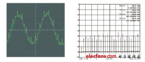
Figure 1: This graph shows the time domain charge injection (single-ended) versus the frequency domain charge injection into the internal sampling capacitor.
Typically, the input impedance of this type of converter is very high (on the order of several thousand Ω) at low frequencies (<100MHz); above 200MHz, the differential input impedance drops to about 200Ω. The same is true for the imaginary (i.e., capacitive) part of the input impedance, which is quite high at low frequencies and tapers off to about 1-2pF at high frequencies. "Matching" this input structure is a very challenging design problem, especially at frequencies above 100MHz.
It is important to use a differential structure at the input, especially for frequency domain design. Differential front-end design provides better common-mode rejection of charge injection and helps in design.
Converters with input buffers are easier to design. The downside is that they consume more power because the buffers must be designed to be highly linear and low noise. The input impedance is usually specified as a fixed differential R||C impedance. It is buffered by a transistor stage that drives the conversion process with low impedance, thus significantly reducing charge injection spikes and switching transients.
Unlike switched capacitor ADCs, the input terminals are almost unchanged during the sample and hold phase of the conversion process. Therefore, the design of the driver circuit is much easier than that of an unbuffered ADC. Figure 2 shows the simplified structure of the internal sample and hold circuit of a buffered and unbuffered ADC.
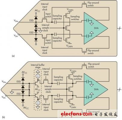
Figure 2: Shown is a comparison of unbuffered (a) and buffered (b) high-speed pipeline ADC sample-and-hold circuits.
Choosing a converter can be difficult, but most designs today are designed to minimize power consumption, so designers often use unbuffered converters. If linearity is more important than power consumption, a buffered converter is often the choice. It should be noted that no matter which converter is chosen, the higher the frequency of the application, the more difficult the front-end design becomes. Choosing a buffered converter alone will not solve all problems. However, in some cases, it may reduce design complexity.
Converter Input Impedance Calculation: Measurement Methods
On the surface, this may seem very tricky, but there are actually several ways to measure the impedance of a converter. The trick is to use a network analyzer to do most of the grunt work, but such equipment can be expensive. The advantage is that today's network analyzers are capable of many functions, such as trace calculation and de-embedding, and for tasks such as impedance conversion, they can give you the answer directly without the need for external software.
Measuring the impedance of a converter requires two circuit boards, a network analyzer, and a little "hacking" knowledge. The first board has the ADC/DUT (device under test) soldered on, along with other components to provide bias and clock (Figure 3a). The second high-speed ADC evaluation board has the front-end circuitry removed, leaving only the traces to the converter's analog input pins (Figure 3b).
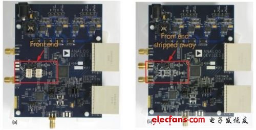
Figure 3: Measuring the impedance of an ADC requires an ADC evaluation board (a) with the front end removed for measurement (b).
The second board removes any parasitics from the routing of the removed front-end circuitry. To do this, a bare board with the same circuitry as that shown in Figure 3b but without the components soldered to it must be used (Figure 4a). This bare board is then cut to leave only the portion where the front-end circuitry routing enters the analog input pins of the ADC (Figure 4b).
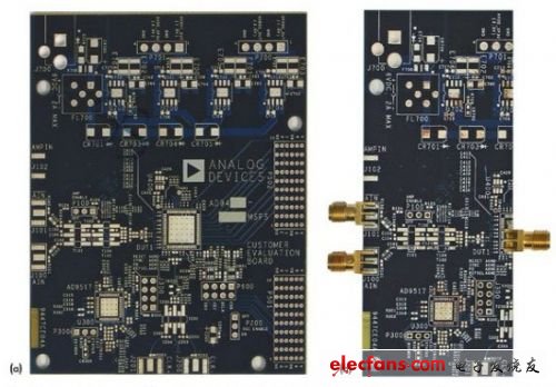
Figure 4: To remove the parasitic effects of the wires from the stripped front-end circuitry, the bare board with no solder components as shown in Figure 3b is used (a). A cut-out version of the board allows only the front-end circuitry wires to connect to the analog input pins of the ADC (b).
A connector needs to be installed at the pins of the converter (usually there is enough copper to do this). Creativity can be used at this stage to ensure a solid connection of this connector. Usually, the exposed pad (epad) of the ADC can be used to make the connection from the converter itself to ground. Assuming that the two differential traces of the front-end circuit are equal and symmetrical, only one of the traces needs to be used. This board is used to make a "through" measurement, and the previous measurement will be subtracted from the measurement of the board with the device soldered on.
The next step is to perform a "through" measurement on the cut-out bare board (the second board shown in Figure 4b) to measure S21 (Figure 5). This file (which should be saved in touchstone format or as a .S2P file) will become the de-embed file used to remove all trace parasitics from the board with the device soldered on it.
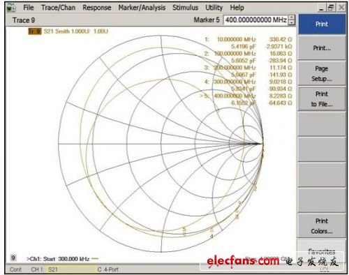
Figure 5: The wire impedance of the shear plate shown in Figure 4b without the front-end circuitry.
Then simply connect the assembly board (the first board shown in Figure 3b) to the network analyzer in a differential configuration. The board should be powered and clocked to ensure that any parasitic changes in the converter’s internal front-end design are captured during the measurement.
After the assembly board is “powered up,” the converter looks like it would in a typical application. In this measurement, the board parasitics previously measured on each port (each analog input trace) of the cut bare board (Figure 6) are removed. The board parasitics will ultimately be subtracted from the current ADC measurement, leaving only the package and internal front-end impedances in the graph (Figure 7).
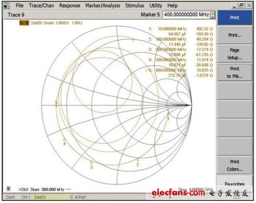
Figure 6: This curve illustrates the ADC impedance without removing the front-end circuit parasitics.
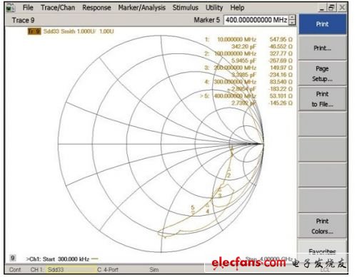
Figure 7: This curve illustrates the impedance of the ADC without the parasitic effects of the front-end circuitry.
Converter Input Impedance Calculation: Mathematical Method
Now let’s do some math to see if the time spent on lab measurements is worth it. The internal input impedance of any converter can be modeled (Figure 8). This network is a good model for describing the ac performance of the input network in tracking mode (i.e., when sampling).
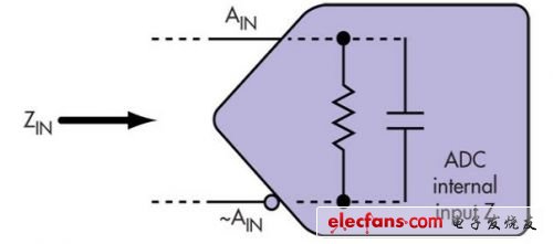
Figure 8: AC performance of the ADC's internal input network in tracking mode (when sampling is implemented).
ADC internal input Z: ADC internal input impedance
Typically, any data sheet will give some form of static differential input impedance, along with R||C values obtained through simulation. The approach described here uses a very simple model in order to obtain a close approximation and simplify the math. Otherwise, if the equivalent impedance model also includes the sampling clock rate and duty cycle, small impedance changes can make the math very difficult.
It should also be noted that these values are a reflection of the ADC's internal circuitry during the sampling process (i.e., the actual sampling of the signal) in track mode. In hold mode, the sampling switch is open and the input front-end circuitry is isolated from the internal sampling process or buffer.
Deriving this simple model (Figure 8) and solving for the real and imaginary parts:
Z0 = R, Z1 = 1/s • C, s = j • 2 • π • f, f = frequency
ZTOTAL = 1/(1/Z0 + 1/Z1) = 1/(1/R + s • C) = 1/((1 + s • R • C)/R)) = R/(1 + s • R•C)
Substitute s and multiply by the complex conjugate:
ZTOTAL = R/(1 + j • 2 • π • f • R • C) = R/(1 + j • 2 • π • f • R • C) • ((1 – j • 2 • π • f • R • C)/(1 – j • 2 • π • f • R • C)) = (R –j • 2 • π • f • R2 • C)/(1 + (2 • π • f • R • C)2)
Find the real part (Real) and the imaginary part (Imag):
ZTOTAL = Real + j • Imag = R/(1 + (2 • π • f • R • C)2) + j • (–2 • π • f • R2 • C)/(1 + 2 • π • f • R • C)2)
Real = R/(1 + (2 • π • f • R • C)2) Imag = (–2 • π • f • R2 • C)/(1 + (2 • π • f • R • C)2 )
This mathematical model agrees very well with the AC simulations in tracking mode (Figures 9 and 10). The main source of error for this simple model is the level at which the impedance settles at high frequencies. Note that these values are generally obtained through a series of simulations and are fairly accurate.
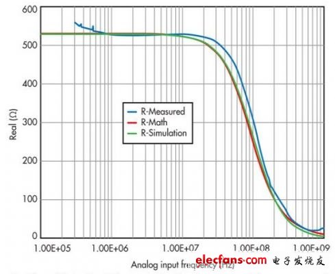
Figure 9: Shown is the “real” portion of the converter input impedance curve, comparing the results obtained by measured, mathematical and simulation methods.
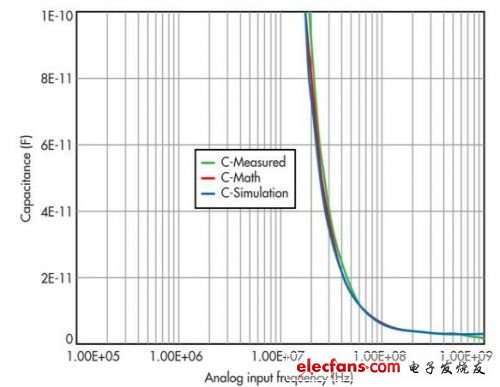
Figure 10: Shown is the “imaginary” portion of the converter input impedance curve, comparing the results obtained by measured, mathematical and simulation methods.
Now let's discuss the measured results shown in Figures 9 and 10. All three curves do not coincide exactly, but they are close, because some measurement errors always exist and the simulation may not take into account all the packaging parasitics of the converter. Therefore, a certain degree of inconsistency is normal. Nevertheless, the curves are very similar in shape and contour, giving a fairly close approximation of the converter's impedance characteristics.
Note that a network analyzer can only provide reliable measurements within a range of its characteristic impedance standard times/divided by 10. If the characteristic impedance of a network analyzer is 50Ω, then satisfactory measurements can only be made within a range of 5Ω to 500Ω. This is one reason why data sheets prefer to list simple R||C values.
ADC Input Impedance Summary
Understanding converter impedance is an important part of signal chain design. In short, why waste a lot of money on expensive test equipment or go through the trouble of measuring impedance if you don’t really need it? It is faster and easier to get the converter impedance curve by using the RC parallel combination impedance provided by the data sheet and a little simple calculation.
Previous article:Steady-state and dynamic test methods for UPS power supply
Next article:Method for measuring half-load internal resistance of battery capacity
- Popular Resources
- Popular amplifiers
-
 Evaluating Roadside Perception for Autonomous Vehicles: Insights from Field Testing
 -
 Chip Manufacturing: A Practical Tutorial on Semiconductor Process Technology (Sixth Edition)
 -
 Handbook of Semiconductor Interconnection Technology
 -
 Beta‐detected Nuclear Magnetic Resonance (β‐NMR) Towards Depth Resolved NMR
- From probes to power supplies, Tektronix is leading the way in comprehensive innovation in power electronics testing
- Seizing the Opportunities in the Chinese Application Market: NI's Challenges and Answers
- Tektronix Launches Breakthrough Power Measurement Tools to Accelerate Innovation as Global Electrification Accelerates
- Not all oscilloscopes are created equal: Why ADCs and low noise floor matter
- Enable TekHSI high-speed interface function to accelerate the remote transmission of waveform data
- How to measure the quality of soft start thyristor
- How to use a multimeter to judge whether a soft starter is good or bad
- What are the advantages and disadvantages of non-contact temperature sensors?
- In what situations are non-contact temperature sensors widely used?
- LED chemical incompatibility test to see which chemicals LEDs can be used with
- Application of ARM9 hardware coprocessor on WinCE embedded motherboard
- What are the key points for selecting rotor flowmeter?
- LM317 high power charger circuit
- A brief analysis of Embest's application and development of embedded medical devices
- Single-phase RC protection circuit
- stm32 PVD programmable voltage monitor
- Introduction and measurement of edge trigger and level trigger of 51 single chip microcomputer
- Improved design of Linux system software shell protection technology
- What to do if the ABB robot protection device stops
- Analysis of the application of several common contact parts in high-voltage connectors of new energy vehicles
- Wiring harness durability test and contact voltage drop test method
- From probes to power supplies, Tektronix is leading the way in comprehensive innovation in power electronics testing
- From probes to power supplies, Tektronix is leading the way in comprehensive innovation in power electronics testing
- Sn-doped CuO nanostructure-based ethanol gas sensor for real-time drunk driving detection in vehicles
- Design considerations for automotive battery wiring harness
- Do you know all the various motors commonly used in automotive electronics?
- What are the functions of the Internet of Vehicles? What are the uses and benefits of the Internet of Vehicles?
- Power Inverter - A critical safety system for electric vehicles
- Analysis of the information security mechanism of AUTOSAR, the automotive embedded software framework
- The impact of water depth on power supply and communications.
- 【CH579M-R1】3. ADC internal temperature measurement, external channel and touch button test
- How to migrate from GCC Linker to SEGGER Linker in Embedded Studio?
- Based on PSOC6 development board simulation I2C solution X-NUCLEO-IKS01A3 LPS22HH
- 【CH579M-R1】+OTA first experience
- I created a project with stm32cubemx and then used the module generated by keil RTE, but the code generated by RTE is repeated. How can I disable the duplication?
- 【ESP32-C3-DevKitM-1】LED PWM for ESP32-C3
- CS8626 pin diagram Filter-free, 50W mono Class D power amplifier HT8696 circuit diagram
- 【NUCLEO-L552ZE Review】+wifi module
- Questions about LM317 circuit

 Evaluating Roadside Perception for Autonomous Vehicles: Insights from Field Testing


 京公网安备 11010802033920号