The data acquisition system is the core part of the digital storage oscilloscope. Under the control of the oscilloscope acquisition control circuit, the data acquisition system quantifies the analog signal to be measured and caches it for the oscilloscope software system to process, calculate and display the data. With the continuous development of computer technology, the performance of high-speed ADC is constantly improving, the real-time performance of powerful DSP signal processing is getting stronger and stronger, and the performance of programmable logic devices is constantly improving, providing a reliable and practical digital platform for the implementation of oscilloscope data acquisition systems. Correspondingly, the sampling rate, storage depth, waveform capture capability, and identification capability of the data acquisition system are also constantly improving. Internationally, oscilloscope companies such as Agilent and Tektronix have dominated the digital storage oscilloscope market, and all have oscilloscopes with real-time sampling rates of tens of Gsps on the market. However, due to the limitations of devices and processes, it is still difficult to realize a truly high-speed and high-resolution data acquisition system in China.
This paper adopts the structural mode of ADC+high-frequency clock circuit+FPGA+DSP to design a digital storage oscilloscope data acquisition system with a real-time sampling rate of 2 Gsps, which provides a reference solution for the development of domestic high-speed and high-resolution data acquisition systems.
1. Selection of key components
The main technical indicators of the DSO data acquisition system are: a) dual input channels work simultaneously, and the maximum real-time sampling rate of each channel reaches 2 Gsps; b) vertical resolution is 8 bits; c) storage depth: 8 MB/CH. The key components of the entire system include ADC, high-frequency clock chip, FPGA, DSP, and SRAM. Through the analysis of the main technical indicators of the target system and the application characteristics of the digital storage oscilloscope, the following series of components are selected. The
data acquisition system requires a maximum real-time sampling rate of 2 Gsps. At the same time, considering the vertical resolution and data output format required by the target system, the analog bandwidth of the oscilloscope, the purchase channel of the device and the cost performance, Atmel's AT84AD001 is selected. AT84AD001 is a dual-channel ADC, each channel has a real-time sampling rate of 1 Gsps. In interleaved mode, the parallel sampling of the dual-channel ADC can achieve a real-time sampling rate of 2 Gsps. Its resolution is 8 bits, and the data output format is LVDS (Low Voltage Differential Signaling). It has 1:1 data output or 1:2 data output mode. In addition, the full power input bandwidth (-3 dB) is 1.5 GHz, and the differential voltage input range is 500 mVVpp.
In addition, it is important that AT84AD001 also has FISDA (Fine Sampling Delay Adjustment on Channel Q) function. By adjusting the sampling time of the Q channel, it effectively avoids the error caused by the duty cycle of the sampling clock not being equal to 50%, and ensures the sampling accuracy.
High-speed and high-precision ADCs have very high requirements for the accuracy of the sampling clock. The general design method of the clock circuit is to directly use the phase-locked loop frequency multiplication circuit inside the FPGA to generate it. However, the target system requires the sampling clock frequency to reach 1 GHz, while the current high-end FPGAs of Altera and Xilinx can only reach a maximum I/O output frequency of 800MHz. After comprehensive evaluation, the high-frequency clock chip LMX2531LQ1910E of NS Company in the United States was finally selected. Its output low-band frequency is 917 MHz to 1 014 MHz, which meets the design requirements. In addition, LMX2531 has very low jitter and phase noise. It also integrates low-noise, high-performance low-dropout linear regulator LDO (Low Drop Out regulator) components, which improves the anti-interference and stability of the circuit. The
programmability of FPGA and its rich internal logic resources and external I/O resources are used as a digital storage oscilloscope data acquisition and control system. In particular, the quantized output of the single-chip AT84AD001 is 16 channels of 1 Gbps rate, LVDS format differential data. The dual input channels of the target system work simultaneously, which requires the FPGA to have 32 differential I/Os that can support 1 Gbps, and use high-speed I/Os to receive and store data. Therefore, Altera's Stratix II EP2S60F1020C4 was selected. This FPGA can support up to 84 1 Gbps differential channels, and adds a dynamic phase alignment circuit for the source synchronous channel, which provides strong support for the reception of high-speed data.
In the high-speed data acquisition system of the oscilloscope, a large amount of real-time calculation and processing of the collected data is required. After comprehensive consideration of various processors on the market, the DSP chip Blackfin561 of ADI was selected as the embedded computing system. The main frequency of Blackfin561 can reach up to 750 MHz. Its core includes two 16-bit multiplier and accumulator MACs, two 40-bit accumulator ALUs, a 40-bit shifter, 100KB of on-chip L1 memory and 128KB of on-chip L2 memory SRAM, and has dynamic power management function. In addition, the Blackfin processor also includes a rich peripheral interface to meet the needs of the design. The
storage depth of the digital storage oscilloscope designed in this paper is required to reach 8 MB per channel, while the on-chip storage unit of the FPGA chip Stratix II EP2S60F1020C4 is only 552 KB in total. Therefore, an off-chip memory must be used as the acquisition RAM to store the quantized waveform data. After comprehensive consideration, the SRAM chip CY7C1440AV33 of Cypress Corporation of the United States was selected.
2 System Structure
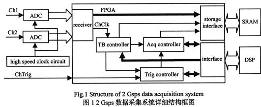
The data acquisition system designed in this paper adopts the structure mode of ADC+high-speed clock circuit+FPGA+SRAM+DSP, and its system structure is shown in Figure 1. Channel 1 and Channel 2 both use an AT84AD001 with a maximum real-time sampling rate of 2 Gsps as an analog-to-digital converter to complete the quantization of the analog input signal. The high-frequency clock circuit is used to generate the working clock required by the entire data acquisition system. The FPGA is used to complete the reception of the sampled data and realize the interface circuit between the FPGA and the DSP; the SRAM is used as the acquisition RAM of the data acquisition system to complete the quantized waveform data cache; the DSP is the main control machine of the data acquisition system to complete the control of the acquisition circuit and receive the data collected by the acquisition circuit, and process, analyze and display the sampled data.
3 Hardware Design
3.1 Design of the high-speed clock circuit of the target system
It is programmed through the standard three-wire serial interface (CLK, DATA, LE) of LMX2531 to control LMX2531 to output the desired frequency. The formula for calculating the clock output frequency is:
fout=N×(OSCin/R) (1)
Where N=Ninteger+Nfractional (including integer and decimal parts), the value of Ninteger is the value of the IV divider, the value of Nfractional includes the values of NUM and DEN, R represents the value of the R divider, and OSCin is the reference clock input value. The value of the R divider can be selected by the user from 1, 2, 4, 8, 16, 32, and the reference clock input OSCin and the output frequency fout are also determined by the user. According to the design requirements, determine the specific values of each register, write the calculated data into the 11 24-bit control registers in the chip, and obtain the 1 GHz clock required by the ADC. [page]
3.2 Setting the AT84AD001 working mode
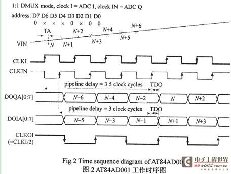
The working sequence of AT84AD001 is shown in Figure 2. Both I and Q channel ADCs use I channel to input analog signals. The working clock frequency of I channel is 1 GHz. The working clock of Q channel is inversely proportional to the working clock of I channel. In this mode, two ADCs with real-time sampling rate of 1 Gsps are sampled in parallel in an alternating manner, and the obtained data is combined into a 2 Gsps data stream according to a certain output format.
3.3 Introduction to FPGA internal logic modules
The internal logic modules of FPGA mainly include:
1) Time base circuit module: Receive the output data of AT84AD001 and synchronously latch the clock as the working clock inside FPGA, and provide a time base scale for the data acquisition system.
2) Data acquisition interface and storage interface module:
FPGA's serial transceiver SERDES (Serializer/Deserializer) and dynamic phase alignment DPA (Dynamic Phase Alignment) circuit are used to receive LVDS format, 1 Gbps differential data stream, and down-convert it. Then, according to the corresponding order of differential channels and ADC data bits and the output format of receiver data, a recovery circuit is designed to restore 64-bit data to 8 sampling points in the format of sampling points. Finally, a data storage interface is established between FPGA and off-chip memory to write data to the off-chip memory at a certain rate and format.
3) Acquisition control module: The acquisition state machine is used to cooperate with the software system to manage the entire acquisition process, and the entire acquisition project is completed according to the set pre-trigger and post-trigger data volume.
4) Trigger control module: It is used to capture signal feature points and synchronize waveform display. 5) Computing
system interface module: Complete the communication between FPGA and DSP.
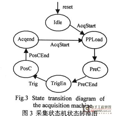
Among them, the acquisition state machine, as the core of the acquisition control module, is responsible for the control of the entire data acquisition process and plays a pivotal role. It is a state machine compiled in VHDL language, and its state transition is shown in Figure 3. The description of the acquisition state involved in the state transition in Figure 3 is shown in Table 1.

4 Data Acquisition System Monitoring Software Design
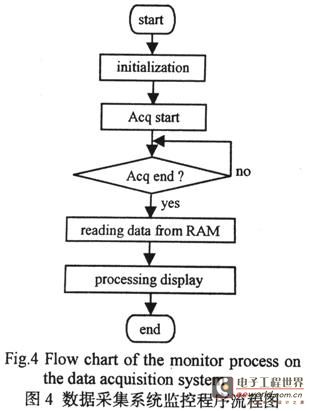
In order to facilitate the testing of the entire hardware, a simple monitoring program is compiled in the DSP, and the program flow chart is shown in Figure 4. First, the DSP calls the initialization program of the clock chip and ADC to complete the initialization of the high-speed clock circuit and the acquisition circuit, so that it works in the working mode required by the target system; then it issues an acquisition start command, and the data acquisition system enters the acquisition process; after a delay, it queries the acquisition end flag; when it is known that the acquisition process is over, it reads the waveform data from the RAM and sends it to the display after analysis and processing. [page]
5 Debugging Results
5.1 Analysis of the real-time sampling rate
is 10 MHz, 150 mvVpp sine wave. The data acquisition system monitoring program is run in the software development environment Visual DSP++ to obtain the sampling data of channel 1 and channel 2. The debugging tool in VDSP uses the sampling data of channel 1 and channel 2 as the data source, and after channel calibration, adjusts the offset and analog signal gain differences between the dual-channel ADCs contained in the analog-to-digital converter of each channel. Select any 400 sampling points to restore the sampling waveform in the form of a line graph, as shown in Figure 5.
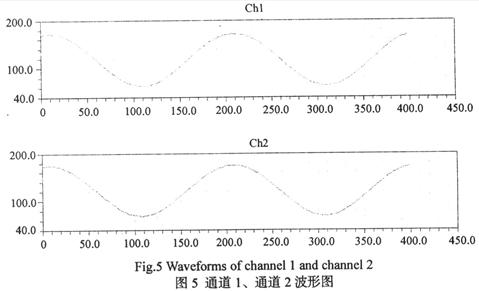
Extracting 400 consecutive sampling points from the acquired waveform data to restore the waveform just shows two signal cycles. In addition, the amplitude of the restored waveform is consistent with the amplitude of the signal source. It can be seen that both channel 1 and channel 2 have achieved a real-time sampling rate of 2 Gsps.
5.2 Analysis of Effective Number of Bits (ENOB)
Effective Number of Bits (ENOB) is one of the most important indicators for measuring the dynamic characteristics of a data acquisition system. The calculation formula is: ENOB = (SINAD-1.16 dB) / 6.02. SINAD is the ratio of the root mean square value of the signal amplitude to the root mean square value of all other spectral components in the bandwidth from DC to fs/2 (including harmonics but excluding DC components). The calculation formula is:

the input signals of channel 1 and channel 2 are both 10 MHz, 330 mVVpp sine waves. Run the data acquisition system monitoring program in VDSP to obtain the sampling data of channel 1 and channel 2. Take any 1 024 consecutive sampling points from the sampling data of each channel as test data. Use Matlab programming to calculate the effective number of bits (ENOB) respectively: 6.71 (channel 1) and 6.77 (channel 2). The above calculation results show that the data acquisition system has a high quantization resolution.
6 Conclusion
Through the hardware debugging and software simulation of the experimental board, a digital oscilloscope data acquisition system with dual channels working simultaneously, a maximum real-time sampling rate of 2 Gsps per channel, a resolution of 8 bits, and a storage depth of 8 MB/CH is designed, and it is verified that the data storage and data storage on the experimental board can meet the requirements of the 2 Gsps data acquisition system.
Keywords:2Gsps
Reference address:Design of a 2Gsps digital oscilloscope data acquisition system
This paper adopts the structural mode of ADC+high-frequency clock circuit+FPGA+DSP to design a digital storage oscilloscope data acquisition system with a real-time sampling rate of 2 Gsps, which provides a reference solution for the development of domestic high-speed and high-resolution data acquisition systems.
1. Selection of key components
The main technical indicators of the DSO data acquisition system are: a) dual input channels work simultaneously, and the maximum real-time sampling rate of each channel reaches 2 Gsps; b) vertical resolution is 8 bits; c) storage depth: 8 MB/CH. The key components of the entire system include ADC, high-frequency clock chip, FPGA, DSP, and SRAM. Through the analysis of the main technical indicators of the target system and the application characteristics of the digital storage oscilloscope, the following series of components are selected. The
data acquisition system requires a maximum real-time sampling rate of 2 Gsps. At the same time, considering the vertical resolution and data output format required by the target system, the analog bandwidth of the oscilloscope, the purchase channel of the device and the cost performance, Atmel's AT84AD001 is selected. AT84AD001 is a dual-channel ADC, each channel has a real-time sampling rate of 1 Gsps. In interleaved mode, the parallel sampling of the dual-channel ADC can achieve a real-time sampling rate of 2 Gsps. Its resolution is 8 bits, and the data output format is LVDS (Low Voltage Differential Signaling). It has 1:1 data output or 1:2 data output mode. In addition, the full power input bandwidth (-3 dB) is 1.5 GHz, and the differential voltage input range is 500 mVVpp.
In addition, it is important that AT84AD001 also has FISDA (Fine Sampling Delay Adjustment on Channel Q) function. By adjusting the sampling time of the Q channel, it effectively avoids the error caused by the duty cycle of the sampling clock not being equal to 50%, and ensures the sampling accuracy.
High-speed and high-precision ADCs have very high requirements for the accuracy of the sampling clock. The general design method of the clock circuit is to directly use the phase-locked loop frequency multiplication circuit inside the FPGA to generate it. However, the target system requires the sampling clock frequency to reach 1 GHz, while the current high-end FPGAs of Altera and Xilinx can only reach a maximum I/O output frequency of 800MHz. After comprehensive evaluation, the high-frequency clock chip LMX2531LQ1910E of NS Company in the United States was finally selected. Its output low-band frequency is 917 MHz to 1 014 MHz, which meets the design requirements. In addition, LMX2531 has very low jitter and phase noise. It also integrates low-noise, high-performance low-dropout linear regulator LDO (Low Drop Out regulator) components, which improves the anti-interference and stability of the circuit. The
programmability of FPGA and its rich internal logic resources and external I/O resources are used as a digital storage oscilloscope data acquisition and control system. In particular, the quantized output of the single-chip AT84AD001 is 16 channels of 1 Gbps rate, LVDS format differential data. The dual input channels of the target system work simultaneously, which requires the FPGA to have 32 differential I/Os that can support 1 Gbps, and use high-speed I/Os to receive and store data. Therefore, Altera's Stratix II EP2S60F1020C4 was selected. This FPGA can support up to 84 1 Gbps differential channels, and adds a dynamic phase alignment circuit for the source synchronous channel, which provides strong support for the reception of high-speed data.
In the high-speed data acquisition system of the oscilloscope, a large amount of real-time calculation and processing of the collected data is required. After comprehensive consideration of various processors on the market, the DSP chip Blackfin561 of ADI was selected as the embedded computing system. The main frequency of Blackfin561 can reach up to 750 MHz. Its core includes two 16-bit multiplier and accumulator MACs, two 40-bit accumulator ALUs, a 40-bit shifter, 100KB of on-chip L1 memory and 128KB of on-chip L2 memory SRAM, and has dynamic power management function. In addition, the Blackfin processor also includes a rich peripheral interface to meet the needs of the design. The
storage depth of the digital storage oscilloscope designed in this paper is required to reach 8 MB per channel, while the on-chip storage unit of the FPGA chip Stratix II EP2S60F1020C4 is only 552 KB in total. Therefore, an off-chip memory must be used as the acquisition RAM to store the quantized waveform data. After comprehensive consideration, the SRAM chip CY7C1440AV33 of Cypress Corporation of the United States was selected.
2 System Structure
The data acquisition system designed in this paper adopts the structure mode of ADC+high-speed clock circuit+FPGA+SRAM+DSP, and its system structure is shown in Figure 1. Channel 1 and Channel 2 both use an AT84AD001 with a maximum real-time sampling rate of 2 Gsps as an analog-to-digital converter to complete the quantization of the analog input signal. The high-frequency clock circuit is used to generate the working clock required by the entire data acquisition system. The FPGA is used to complete the reception of the sampled data and realize the interface circuit between the FPGA and the DSP; the SRAM is used as the acquisition RAM of the data acquisition system to complete the quantized waveform data cache; the DSP is the main control machine of the data acquisition system to complete the control of the acquisition circuit and receive the data collected by the acquisition circuit, and process, analyze and display the sampled data.

3 Hardware Design
3.1 Design of the high-speed clock circuit of the target system
It is programmed through the standard three-wire serial interface (CLK, DATA, LE) of LMX2531 to control LMX2531 to output the desired frequency. The formula for calculating the clock output frequency is:
fout=N×(OSCin/R) (1)
Where N=Ninteger+Nfractional (including integer and decimal parts), the value of Ninteger is the value of the IV divider, the value of Nfractional includes the values of NUM and DEN, R represents the value of the R divider, and OSCin is the reference clock input value. The value of the R divider can be selected by the user from 1, 2, 4, 8, 16, 32, and the reference clock input OSCin and the output frequency fout are also determined by the user. According to the design requirements, determine the specific values of each register, write the calculated data into the 11 24-bit control registers in the chip, and obtain the 1 GHz clock required by the ADC. [page]
3.2 Setting the AT84AD001 working mode
The working sequence of AT84AD001 is shown in Figure 2. Both I and Q channel ADCs use I channel to input analog signals. The working clock frequency of I channel is 1 GHz. The working clock of Q channel is inversely proportional to the working clock of I channel. In this mode, two ADCs with real-time sampling rate of 1 Gsps are sampled in parallel in an alternating manner, and the obtained data is combined into a 2 Gsps data stream according to a certain output format.

3.3 Introduction to FPGA internal logic modules
The internal logic modules of FPGA mainly include:
1) Time base circuit module: Receive the output data of AT84AD001 and synchronously latch the clock as the working clock inside FPGA, and provide a time base scale for the data acquisition system.
2) Data acquisition interface and storage interface module:
FPGA's serial transceiver SERDES (Serializer/Deserializer) and dynamic phase alignment DPA (Dynamic Phase Alignment) circuit are used to receive LVDS format, 1 Gbps differential data stream, and down-convert it. Then, according to the corresponding order of differential channels and ADC data bits and the output format of receiver data, a recovery circuit is designed to restore 64-bit data to 8 sampling points in the format of sampling points. Finally, a data storage interface is established between FPGA and off-chip memory to write data to the off-chip memory at a certain rate and format.
3) Acquisition control module: The acquisition state machine is used to cooperate with the software system to manage the entire acquisition process, and the entire acquisition project is completed according to the set pre-trigger and post-trigger data volume.
4) Trigger control module: It is used to capture signal feature points and synchronize waveform display. 5) Computing
system interface module: Complete the communication between FPGA and DSP.

Among them, the acquisition state machine, as the core of the acquisition control module, is responsible for the control of the entire data acquisition process and plays a pivotal role. It is a state machine compiled in VHDL language, and its state transition is shown in Figure 3. The description of the acquisition state involved in the state transition in Figure 3 is shown in Table 1.

4 Data Acquisition System Monitoring Software Design
In order to facilitate the testing of the entire hardware, a simple monitoring program is compiled in the DSP, and the program flow chart is shown in Figure 4. First, the DSP calls the initialization program of the clock chip and ADC to complete the initialization of the high-speed clock circuit and the acquisition circuit, so that it works in the working mode required by the target system; then it issues an acquisition start command, and the data acquisition system enters the acquisition process; after a delay, it queries the acquisition end flag; when it is known that the acquisition process is over, it reads the waveform data from the RAM and sends it to the display after analysis and processing. [page]

5 Debugging Results
5.1 Analysis of the real-time sampling rate
is 10 MHz, 150 mvVpp sine wave. The data acquisition system monitoring program is run in the software development environment Visual DSP++ to obtain the sampling data of channel 1 and channel 2. The debugging tool in VDSP uses the sampling data of channel 1 and channel 2 as the data source, and after channel calibration, adjusts the offset and analog signal gain differences between the dual-channel ADCs contained in the analog-to-digital converter of each channel. Select any 400 sampling points to restore the sampling waveform in the form of a line graph, as shown in Figure 5.

Extracting 400 consecutive sampling points from the acquired waveform data to restore the waveform just shows two signal cycles. In addition, the amplitude of the restored waveform is consistent with the amplitude of the signal source. It can be seen that both channel 1 and channel 2 have achieved a real-time sampling rate of 2 Gsps.
5.2 Analysis of Effective Number of Bits (ENOB)
Effective Number of Bits (ENOB) is one of the most important indicators for measuring the dynamic characteristics of a data acquisition system. The calculation formula is: ENOB = (SINAD-1.16 dB) / 6.02. SINAD is the ratio of the root mean square value of the signal amplitude to the root mean square value of all other spectral components in the bandwidth from DC to fs/2 (including harmonics but excluding DC components). The calculation formula is:

the input signals of channel 1 and channel 2 are both 10 MHz, 330 mVVpp sine waves. Run the data acquisition system monitoring program in VDSP to obtain the sampling data of channel 1 and channel 2. Take any 1 024 consecutive sampling points from the sampling data of each channel as test data. Use Matlab programming to calculate the effective number of bits (ENOB) respectively: 6.71 (channel 1) and 6.77 (channel 2). The above calculation results show that the data acquisition system has a high quantization resolution.
6 Conclusion
Through the hardware debugging and software simulation of the experimental board, a digital oscilloscope data acquisition system with dual channels working simultaneously, a maximum real-time sampling rate of 2 Gsps per channel, a resolution of 8 bits, and a storage depth of 8 MB/CH is designed, and it is verified that the data storage and data storage on the experimental board can meet the requirements of the 2 Gsps data acquisition system.
Previous article:Design of FIR digital filter based on CPLD
Next article:Application of Conducted Noise Analysis Technology in Filters
- Popular Resources
- Popular amplifiers
Recommended Content
Latest Test Measurement Articles
- Seizing the Opportunities in the Chinese Application Market: NI's Challenges and Answers
- Tektronix Launches Breakthrough Power Measurement Tools to Accelerate Innovation as Global Electrification Accelerates
- Not all oscilloscopes are created equal: Why ADCs and low noise floor matter
- Enable TekHSI high-speed interface function to accelerate the remote transmission of waveform data
- How to measure the quality of soft start thyristor
- How to use a multimeter to judge whether a soft starter is good or bad
- What are the advantages and disadvantages of non-contact temperature sensors?
- In what situations are non-contact temperature sensors widely used?
- How non-contact temperature sensors measure internal temperature
MoreSelected Circuit Diagrams
MorePopular Articles
- LED chemical incompatibility test to see which chemicals LEDs can be used with
- Application of ARM9 hardware coprocessor on WinCE embedded motherboard
- What are the key points for selecting rotor flowmeter?
- LM317 high power charger circuit
- A brief analysis of Embest's application and development of embedded medical devices
- Single-phase RC protection circuit
- stm32 PVD programmable voltage monitor
- Introduction and measurement of edge trigger and level trigger of 51 single chip microcomputer
- Improved design of Linux system software shell protection technology
- What to do if the ABB robot protection device stops
MoreDaily News
- Detailed explanation of intelligent car body perception system
- How to solve the problem that the servo drive is not enabled
- Why does the servo drive not power on?
- What point should I connect to when the servo is turned on?
- How to turn on the internal enable of Panasonic servo drive?
- What is the rigidity setting of Panasonic servo drive?
- How to change the inertia ratio of Panasonic servo drive
- What is the inertia ratio of the servo motor?
- Is it better for the motor to have a large or small moment of inertia?
- What is the difference between low inertia and high inertia of servo motors?
Guess you like
- The most detailed summary of embedded system knowledge and interface technology ever!
- Problems with current sinking and current sourcing of the I/O port of the msp430 microcontroller
- Newbie help, how to modify the contents of a file with the suffix bin
- From fail to pass, what does DDR debugging go through?
- [Mil MYS-8MMX] Part 1: Unboxing~
- How to keep one decimal place in C language
- Common problems and solutions in CCS compilation
- First week of SensorTile.box initial experiment
- [Fudan Micro FM33LC046N] FLASH basic time simple test
- EEWORLD University Hall----POS Printer/Printer Special

 TC52N3143ECTRT


 京公网安备 11010802033920号