Digital balances are among the most accurate analog instruments. They use force sensors to detect the weight of an object. Balances are used in a wide variety of applications, from point-of-sale terminals to industrial measurement equipment.
The most common design for a balance is to configure a resistive load cell as a Wheatstone bridge. However, the interface to the sensor is complex due to the high accuracy required. In a load cell, the signal level is low, making noise a significant factor. This article will discuss how to accurately measure the signal to meet the precision measurement needs of a balance. It will also explore the different parameters of the load cell and how they affect accuracy. A balance system is not only an analog front end (AFE) for high-precision measurements, but also requires a clear user interface and a voltage boost circuit to handle low battery issues. In addition, for some balances, it is necessary to communicate with a host controller via a communication protocol. Other factors to consider include cost management issues and how to integrate all of the above features into the balance design.
Analog Front End
Let's first look at the analog front end of a balance. Figure 1 shows the basic layout of an analog front end for a balance application.
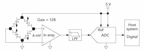
Figure 1: Analog front end of a scale
In this arrangement, the sensor output signal is first amplified and then filtered to remove noise from the power supply and mechanical vibration. The filtered output signal is sampled by a high-resolution ADC. A load cell is a resistive sensor that provides a voltage proportional to the applied load. The most commonly used load cells consist of several strain gauges connected in a Wheatstone bridge. Figure 2 shows the basic arrangement of the strain gauges that make up a load cell in a Wheatstone bridge.
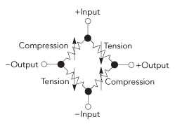
Figure 2: Full-bridge load cell configuration
This is the full-bridge layout of the load cell, also known as the fully active state, where all arms have strain gauges and react to output changes, two of which undergo positive changes in tension, and the other two undergo positive changes in compression. Thus, when pressure is applied to the sensor, the resistance of two of the sensors increases and the resistance of the other two decreases. The change in resistance causes the bridge to be unbalanced, resulting in a differential output corresponding to the weight applied.
Load cells have some specific parameters related to their properties, depending on their construction, materials, and design. These parameters must be understood before designing a load cell interface.
Sensitivity (rated output): This is one of the most important parameters of a load cell. The sensitivity of a load cell is defined as the ratio of the full-load output voltage to the excitation voltage, usually in units of mV/V. This value corresponds to the voltage deviation produced by the load cell under full load conditions with an excitation voltage of 1V. The sensitivity of a load cell is very low, usually only 2mV/V. If the excitation voltage of the system is 3.3V, the output voltage under full load is 6.6mV. Therefore, it is necessary to equip the load cell with a high-precision ADC.
Nonlinearity: As a mechanical device, the load cell has nonlinear characteristics due to its own construction. The nonlinearity of the load cell is generally around 0.015% of the rated output, which is equivalent to 1 bit (when the ADC samples at 13 bits). However, we must remember that the nonlinearity introduced by the load cell is only part of the overall system nonlinearity, and the measurement system and analog front end also have an impact on the overall nonlinearity of the system.
Hysteresis: Hysteresis error is the difference between the output value of the load cell when a lighter weight and a heavier weight are used to achieve a specific load. This is caused by the deformation properties of the load cell material. The higher weight may temporarily cause the load cell to deform, and when the target load is reached, the deviation caused by the deformation will affect the output of the load cell.
Repeatability: refers to the change in the load value measured by the load cell when the same weight is placed on the same load cell multiple times.
Creep and creep recovery: Creep refers to the change in the measured weight over time, such as when the measured object is left on the scale for a long time. For example, the output value will change when the object is placed on the balance and 30 minutes later. This phenomenon is caused by the elastic properties of the material used in the load cell. Cheap materials have large creep values and the load cell takes a long time to recover from deformation.
System Accuracy
Most balance designers use two different resolutions, display resolution and internal resolution. Display resolution refers to the resolution of the final measurement result displayed by the balance, while internal resolution is the actual resolution of the internal analog front end.
Let's assume that the balance's load cell excitation voltage is 5V and the sensitivity is 2mV/V, so the output voltage should be 0-10mV. To set the balance's resolution to 5 grams and the weighing range to 10 kg, the balance's display resolution is 1:2000. As mentioned earlier, the balance's display resolution is different from the internal resolution, which is usually 20 to 30 times the display resolution. Therefore, for this balance, the internal resolution should be 1:60000, which is equivalent to 16-bit internal resolution.
As we have discussed before, there are several types of sensor errors that can occur in the load cell interface, starting with the sensor's own errors. Therefore, the internal resolution needs to be higher than the display resolution so that the error effects can be compensated with a higher resolution.
The design solution requires 16-bit resolution to resolve a 10mV input. To measure the full 10mV output, the most common approach is to use a gain stage to amplify the input signal to meet the ADC's input range requirements, as shown in Figure 1, so that more bits can be resolved in a smaller range. For example, to achieve a 10mV measurement range with a 1V range ADC, the user should use an amplifier gain stage to amplify the signal by nearly 100 times.
Let's assume that the ADC resolution is 20 bits and the input range is 1V. The smallest input change that this ADC can resolve is 1uV. Before the signal is input to the ADC, the gain stage is used to amplify the signal to 0-10mV, at which point the minimum resolved voltage is only 10nV. This resolution makes the signal very susceptible to noise. The gain stage amplifies the noise while amplifying the signal. The noise makes a large number of ADC bits unusable, reducing the effective number of bits (ENOB). Therefore, designers must select an ADC with the best ENOB for the required gain setting.
The most commonly used ADC for measuring the output of a load cell is the DeltaSigma (DelSig) ADC. This ADC uses a signal oversampling technique and then slicing it by one tenth to achieve higher resolution. This architecture makes the ADC inherently low-pass, which helps reduce the effects of noise.
Using a good ADC is only half the problem. The other half is the gain stage. Most designs use an external low-noise amplifier. There are products on the market that implement the gain stage within the input stage of the ADC, such as Cypress's PSoC3 and PSoC5. This is done by integrating an input buffer at the ADC input of the PSoC to achieve a gain of up to 8 times. The modulation stage of the ADC itself can also achieve a gain of up to 16 bits. Since no external amplifier stage is required, there is no amplifier noise effect, so the ADC can provide about 18 effective bits. However, for balance applications, resolution is usually referred to as peak-to-peak resolution, which is the effective peak-to-peak resolution calculated after the system removes the effects of noise.
Commercial applications usually require 16 bits of peak-to-peak resolution while being able to measure the entire 10mV input range. The main issue is dealing with system noise, which reduces the effective resolution.
Another major issue with load cell interfaces is the potential for gain error due to the dependence of the output signal range on the excitation voltage. Any change in the excitation voltage will cause a gain error of a similar percentage in the measured value. This problem can be avoided if the signal measurement is calculated as a ratio of the excitation voltage. There are two ways to do this:
1) We can measure the signal and excitation voltage separately and calculate the ratio to remove the gain error. However, this method requires multiplexing the ADC between the two signals. Another problem with this method is that the signal we are detecting is in the 10mV range, while the excitation voltage is in the range of several volts. This requires dynamically changing the gain setting and ADC range parameters, which is not advisable in most analog systems. In addition, dynamically changing parameters will cause mismatches between the two independent measurements. [page]
2) Another approach is to use the reference of the ADC itself, as shown in Figure 3. ADCs usually have pins for connecting external references. The input range of the ADC is defined as a factor of the reference voltage. In this way, every measurement in the ADC is relative to the reference voltage. If we use the excitation voltage or the derivative of the excitation voltage as the ADC reference, we can measure the signal ratiometrically. Since the load measurement of a load cell is proportional to the resistance, this approach is most suitable. In addition, any changes in the excitation voltage can be ignored in the measurement because the ADC reference will be affected in the same way.
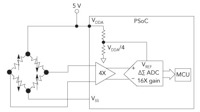
Figure 3: Load Cell Interface Circuit for Ratiometric Measurements
Noise Reduction of Delta Sigma ADCs
The frequency response of the DelSig ADC has some redundancy that can be exploited to reduce noise. The DelSig ADC is an averaging ADC with a low-pass characteristic that significantly reduces noise, as we have discussed previously. However, most DelSig ADCs have a specific frequency response, such as the Sinc response of the PSoC3 and PSoC5 ADCs. This response has nulls at specific frequencies (multiples of the sampling frequency). This
allows us to match the ADC sampling frequency to a specific value, thereby eliminating specific noise bands. This is particularly useful when removing noise sources such as 50/60Hz.
Further Discussion on Filtering - Sliding Average Filtering
We have discussed how to avoid noise and other error sources in the analog signal chain of a scale design. The final step to achieve a noise-free output is to remove the noise using a firmware-based mathematical averaging filter. We introduce a sliding average filter that is easy to implement in Figure 4. It is in the form of an array, with input values flowing in on one side and the oldest values sliding out on the other side. At any given time, the output of the filter is always the average of all elements in the array.
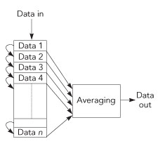
Figure 4: Moving Average Filter
The sliding average filter is the simplest and most effective filtering method that allows the measurement system to achieve a higher noise-free rate. Note that the filter introduces a constant delay that is proportional to the depth of the array. This means that for a sliding filter with n elements, each change will take n cycles to appear in the output. This can be misleading if the change is large and the output reacts slowly. This can be avoided by setting a threshold for the change. For example, if the input changes by more than a threshold within a certain time, the entire filter is cleared and the new data is copied into the filter and copied to the output, which greatly reduces the delay when large changes occur. The size of the filter is selected based on the required resolution, ADC sampling rate, and response time specifications of the balance.
System Design and Integration
Now that we have discussed the analog front-end design and the many considerations for improving performance, the entire balance solution is more than just the analog front-end. Every balance design will use a variety of essential components such as communication interfaces and user interfaces depending on the specific application requirements. Figure 5 shows a typical implementation diagram of a balance solution.
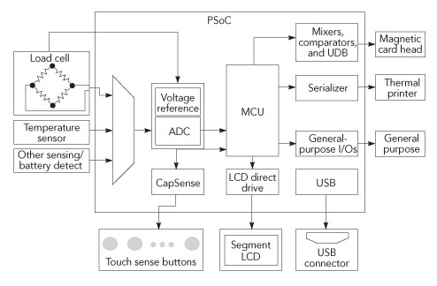
Figure 5: Integrated scale solution based on Cypress PSoC 3 device
In addition to implementing the analog front end for the weighing sensor, the system may also need to measure other analog sensors. Some high-precision scales require temperature monitoring to compensate for the drift of the weighing sensor due to temperature, which means implementing a thermistor interface. If the entire solution is to be portable, a battery charger interface is required, in which case an ADC is required for voltage and current monitoring, as well as separate overvoltage comparators and current protection circuits. There are some dedicated devices on the market to provide battery charging functions, but these functions can be integrated into programmable device SOCs such as PSoC3.
For the user interface, the input method can be a simple touch button. As touch technology develops, some designs can consider using capacitive sensing interfaces. In addition, the output can use LCD technology, but for cost reasons, most designs use direct drive of the LCD to avoid the cost of the LCD driver. The
communication interface can be a simple USB to host processor link or a connection from SPI/I2C to another wireless communication device. The integration of these interfaces can greatly reduce the system cost.
So far, we have discussed the basic components required for most designs. However, some scales, such as those used in point-of-sale terminals, also need to integrate thermal printers and magnetic card reading interfaces. Thermal printers use serializers similar to SPI interfaces, motor drive circuits, analog components for measuring header temperature, and printer paper sensors. Many programmable SoCs provide programmable digital arrays that can integrate thermal printer interfaces programmatically.
Magnetic card is another complex analog function that is usually implemented using an ASIC platform. If this function can also be integrated into the SOC, the BOM cost can be greatly reduced, and Cypress PSoC3 has successfully done this. The programmability of the SoC allows different resources to be reconfigured at run time, such as ADC specifications (input range, resolution, etc.), and connections between different peripherals. In a scale application, all operations—measurement, printing, and card reading—are not performed at the same time. Therefore, all resources on the chip can be shared in time periods, making the design very small and low-cost. The
scale system is one of the measurement systems with the highest accuracy requirements. Due to the high reliability requirements, designers need to understand the basic elements of the weighing sensor, identify the various error sources in the system, and find the specific specifications required for the analog front end, including ADC, amplifier, and filter specifications. Delta Sigma ADC is the best ADC type for this application because of its inherent LFP response, which can effectively resolve high frequency noise and can cope with power supply noise by adjusting the sampling rate. The built-in gain stage in the ADC can reduce the overall system noise and significantly improve ENOB compared to using an external gain stage. In addition, we need to use firmware-based filters (i.e., sliding average filters) to further reduce noise. Other components required in the system include user interface (buttons, LCD, etc.), communication interface (USB, UARTv, etc.), and temperature sensing. Therefore, SoC is the most suitable for this application, which can achieve highly integrated and low-cost solutions and fully meet the requirements of the current competitive market. SoC can also integrate other solutions such as thermal printers and card readers on the same chip.
Reference address:Design of digital scale
The most common design for a balance is to configure a resistive load cell as a Wheatstone bridge. However, the interface to the sensor is complex due to the high accuracy required. In a load cell, the signal level is low, making noise a significant factor. This article will discuss how to accurately measure the signal to meet the precision measurement needs of a balance. It will also explore the different parameters of the load cell and how they affect accuracy. A balance system is not only an analog front end (AFE) for high-precision measurements, but also requires a clear user interface and a voltage boost circuit to handle low battery issues. In addition, for some balances, it is necessary to communicate with a host controller via a communication protocol. Other factors to consider include cost management issues and how to integrate all of the above features into the balance design.
Analog Front End
Let's first look at the analog front end of a balance. Figure 1 shows the basic layout of an analog front end for a balance application.

Figure 1: Analog front end of a scale
In this arrangement, the sensor output signal is first amplified and then filtered to remove noise from the power supply and mechanical vibration. The filtered output signal is sampled by a high-resolution ADC. A load cell is a resistive sensor that provides a voltage proportional to the applied load. The most commonly used load cells consist of several strain gauges connected in a Wheatstone bridge. Figure 2 shows the basic arrangement of the strain gauges that make up a load cell in a Wheatstone bridge.

Figure 2: Full-bridge load cell configuration
This is the full-bridge layout of the load cell, also known as the fully active state, where all arms have strain gauges and react to output changes, two of which undergo positive changes in tension, and the other two undergo positive changes in compression. Thus, when pressure is applied to the sensor, the resistance of two of the sensors increases and the resistance of the other two decreases. The change in resistance causes the bridge to be unbalanced, resulting in a differential output corresponding to the weight applied.
Load cells have some specific parameters related to their properties, depending on their construction, materials, and design. These parameters must be understood before designing a load cell interface.
Sensitivity (rated output): This is one of the most important parameters of a load cell. The sensitivity of a load cell is defined as the ratio of the full-load output voltage to the excitation voltage, usually in units of mV/V. This value corresponds to the voltage deviation produced by the load cell under full load conditions with an excitation voltage of 1V. The sensitivity of a load cell is very low, usually only 2mV/V. If the excitation voltage of the system is 3.3V, the output voltage under full load is 6.6mV. Therefore, it is necessary to equip the load cell with a high-precision ADC.
Nonlinearity: As a mechanical device, the load cell has nonlinear characteristics due to its own construction. The nonlinearity of the load cell is generally around 0.015% of the rated output, which is equivalent to 1 bit (when the ADC samples at 13 bits). However, we must remember that the nonlinearity introduced by the load cell is only part of the overall system nonlinearity, and the measurement system and analog front end also have an impact on the overall nonlinearity of the system.
Hysteresis: Hysteresis error is the difference between the output value of the load cell when a lighter weight and a heavier weight are used to achieve a specific load. This is caused by the deformation properties of the load cell material. The higher weight may temporarily cause the load cell to deform, and when the target load is reached, the deviation caused by the deformation will affect the output of the load cell.
Repeatability: refers to the change in the load value measured by the load cell when the same weight is placed on the same load cell multiple times.
Creep and creep recovery: Creep refers to the change in the measured weight over time, such as when the measured object is left on the scale for a long time. For example, the output value will change when the object is placed on the balance and 30 minutes later. This phenomenon is caused by the elastic properties of the material used in the load cell. Cheap materials have large creep values and the load cell takes a long time to recover from deformation.
System Accuracy
Most balance designers use two different resolutions, display resolution and internal resolution. Display resolution refers to the resolution of the final measurement result displayed by the balance, while internal resolution is the actual resolution of the internal analog front end.
Let's assume that the balance's load cell excitation voltage is 5V and the sensitivity is 2mV/V, so the output voltage should be 0-10mV. To set the balance's resolution to 5 grams and the weighing range to 10 kg, the balance's display resolution is 1:2000. As mentioned earlier, the balance's display resolution is different from the internal resolution, which is usually 20 to 30 times the display resolution. Therefore, for this balance, the internal resolution should be 1:60000, which is equivalent to 16-bit internal resolution.
As we have discussed before, there are several types of sensor errors that can occur in the load cell interface, starting with the sensor's own errors. Therefore, the internal resolution needs to be higher than the display resolution so that the error effects can be compensated with a higher resolution.
The design solution requires 16-bit resolution to resolve a 10mV input. To measure the full 10mV output, the most common approach is to use a gain stage to amplify the input signal to meet the ADC's input range requirements, as shown in Figure 1, so that more bits can be resolved in a smaller range. For example, to achieve a 10mV measurement range with a 1V range ADC, the user should use an amplifier gain stage to amplify the signal by nearly 100 times.
Let's assume that the ADC resolution is 20 bits and the input range is 1V. The smallest input change that this ADC can resolve is 1uV. Before the signal is input to the ADC, the gain stage is used to amplify the signal to 0-10mV, at which point the minimum resolved voltage is only 10nV. This resolution makes the signal very susceptible to noise. The gain stage amplifies the noise while amplifying the signal. The noise makes a large number of ADC bits unusable, reducing the effective number of bits (ENOB). Therefore, designers must select an ADC with the best ENOB for the required gain setting.
The most commonly used ADC for measuring the output of a load cell is the DeltaSigma (DelSig) ADC. This ADC uses a signal oversampling technique and then slicing it by one tenth to achieve higher resolution. This architecture makes the ADC inherently low-pass, which helps reduce the effects of noise.
Using a good ADC is only half the problem. The other half is the gain stage. Most designs use an external low-noise amplifier. There are products on the market that implement the gain stage within the input stage of the ADC, such as Cypress's PSoC3 and PSoC5. This is done by integrating an input buffer at the ADC input of the PSoC to achieve a gain of up to 8 times. The modulation stage of the ADC itself can also achieve a gain of up to 16 bits. Since no external amplifier stage is required, there is no amplifier noise effect, so the ADC can provide about 18 effective bits. However, for balance applications, resolution is usually referred to as peak-to-peak resolution, which is the effective peak-to-peak resolution calculated after the system removes the effects of noise.
Commercial applications usually require 16 bits of peak-to-peak resolution while being able to measure the entire 10mV input range. The main issue is dealing with system noise, which reduces the effective resolution.
Another major issue with load cell interfaces is the potential for gain error due to the dependence of the output signal range on the excitation voltage. Any change in the excitation voltage will cause a gain error of a similar percentage in the measured value. This problem can be avoided if the signal measurement is calculated as a ratio of the excitation voltage. There are two ways to do this:
1) We can measure the signal and excitation voltage separately and calculate the ratio to remove the gain error. However, this method requires multiplexing the ADC between the two signals. Another problem with this method is that the signal we are detecting is in the 10mV range, while the excitation voltage is in the range of several volts. This requires dynamically changing the gain setting and ADC range parameters, which is not advisable in most analog systems. In addition, dynamically changing parameters will cause mismatches between the two independent measurements. [page]
2) Another approach is to use the reference of the ADC itself, as shown in Figure 3. ADCs usually have pins for connecting external references. The input range of the ADC is defined as a factor of the reference voltage. In this way, every measurement in the ADC is relative to the reference voltage. If we use the excitation voltage or the derivative of the excitation voltage as the ADC reference, we can measure the signal ratiometrically. Since the load measurement of a load cell is proportional to the resistance, this approach is most suitable. In addition, any changes in the excitation voltage can be ignored in the measurement because the ADC reference will be affected in the same way.

Figure 3: Load Cell Interface Circuit for Ratiometric Measurements
Noise Reduction of Delta Sigma ADCs
The frequency response of the DelSig ADC has some redundancy that can be exploited to reduce noise. The DelSig ADC is an averaging ADC with a low-pass characteristic that significantly reduces noise, as we have discussed previously. However, most DelSig ADCs have a specific frequency response, such as the Sinc response of the PSoC3 and PSoC5 ADCs. This response has nulls at specific frequencies (multiples of the sampling frequency). This
allows us to match the ADC sampling frequency to a specific value, thereby eliminating specific noise bands. This is particularly useful when removing noise sources such as 50/60Hz.
Further Discussion on Filtering - Sliding Average Filtering
We have discussed how to avoid noise and other error sources in the analog signal chain of a scale design. The final step to achieve a noise-free output is to remove the noise using a firmware-based mathematical averaging filter. We introduce a sliding average filter that is easy to implement in Figure 4. It is in the form of an array, with input values flowing in on one side and the oldest values sliding out on the other side. At any given time, the output of the filter is always the average of all elements in the array.

Figure 4: Moving Average Filter
The sliding average filter is the simplest and most effective filtering method that allows the measurement system to achieve a higher noise-free rate. Note that the filter introduces a constant delay that is proportional to the depth of the array. This means that for a sliding filter with n elements, each change will take n cycles to appear in the output. This can be misleading if the change is large and the output reacts slowly. This can be avoided by setting a threshold for the change. For example, if the input changes by more than a threshold within a certain time, the entire filter is cleared and the new data is copied into the filter and copied to the output, which greatly reduces the delay when large changes occur. The size of the filter is selected based on the required resolution, ADC sampling rate, and response time specifications of the balance.
System Design and Integration
Now that we have discussed the analog front-end design and the many considerations for improving performance, the entire balance solution is more than just the analog front-end. Every balance design will use a variety of essential components such as communication interfaces and user interfaces depending on the specific application requirements. Figure 5 shows a typical implementation diagram of a balance solution.

Figure 5: Integrated scale solution based on Cypress PSoC 3 device
In addition to implementing the analog front end for the weighing sensor, the system may also need to measure other analog sensors. Some high-precision scales require temperature monitoring to compensate for the drift of the weighing sensor due to temperature, which means implementing a thermistor interface. If the entire solution is to be portable, a battery charger interface is required, in which case an ADC is required for voltage and current monitoring, as well as separate overvoltage comparators and current protection circuits. There are some dedicated devices on the market to provide battery charging functions, but these functions can be integrated into programmable device SOCs such as PSoC3.
For the user interface, the input method can be a simple touch button. As touch technology develops, some designs can consider using capacitive sensing interfaces. In addition, the output can use LCD technology, but for cost reasons, most designs use direct drive of the LCD to avoid the cost of the LCD driver. The
communication interface can be a simple USB to host processor link or a connection from SPI/I2C to another wireless communication device. The integration of these interfaces can greatly reduce the system cost.
So far, we have discussed the basic components required for most designs. However, some scales, such as those used in point-of-sale terminals, also need to integrate thermal printers and magnetic card reading interfaces. Thermal printers use serializers similar to SPI interfaces, motor drive circuits, analog components for measuring header temperature, and printer paper sensors. Many programmable SoCs provide programmable digital arrays that can integrate thermal printer interfaces programmatically.
Magnetic card is another complex analog function that is usually implemented using an ASIC platform. If this function can also be integrated into the SOC, the BOM cost can be greatly reduced, and Cypress PSoC3 has successfully done this. The programmability of the SoC allows different resources to be reconfigured at run time, such as ADC specifications (input range, resolution, etc.), and connections between different peripherals. In a scale application, all operations—measurement, printing, and card reading—are not performed at the same time. Therefore, all resources on the chip can be shared in time periods, making the design very small and low-cost. The
scale system is one of the measurement systems with the highest accuracy requirements. Due to the high reliability requirements, designers need to understand the basic elements of the weighing sensor, identify the various error sources in the system, and find the specific specifications required for the analog front end, including ADC, amplifier, and filter specifications. Delta Sigma ADC is the best ADC type for this application because of its inherent LFP response, which can effectively resolve high frequency noise and can cope with power supply noise by adjusting the sampling rate. The built-in gain stage in the ADC can reduce the overall system noise and significantly improve ENOB compared to using an external gain stage. In addition, we need to use firmware-based filters (i.e., sliding average filters) to further reduce noise. Other components required in the system include user interface (buttons, LCD, etc.), communication interface (USB, UARTv, etc.), and temperature sensing. Therefore, SoC is the most suitable for this application, which can achieve highly integrated and low-cost solutions and fully meet the requirements of the current competitive market. SoC can also integrate other solutions such as thermal printers and card readers on the same chip.
Previous article:Comparing SCPI and ICL commands and scripts
Next article:TI energy measurement IC simplifies submetering
- Popular Resources
- Popular amplifiers
Recommended Content
Latest Test Measurement Articles
- From probes to power supplies, Tektronix is leading the way in comprehensive innovation in power electronics testing
- Seizing the Opportunities in the Chinese Application Market: NI's Challenges and Answers
- Tektronix Launches Breakthrough Power Measurement Tools to Accelerate Innovation as Global Electrification Accelerates
- Not all oscilloscopes are created equal: Why ADCs and low noise floor matter
- Enable TekHSI high-speed interface function to accelerate the remote transmission of waveform data
- How to measure the quality of soft start thyristor
- How to use a multimeter to judge whether a soft starter is good or bad
- What are the advantages and disadvantages of non-contact temperature sensors?
- In what situations are non-contact temperature sensors widely used?
MoreSelected Circuit Diagrams
MorePopular Articles
- LED chemical incompatibility test to see which chemicals LEDs can be used with
- Application of ARM9 hardware coprocessor on WinCE embedded motherboard
- What are the key points for selecting rotor flowmeter?
- LM317 high power charger circuit
- A brief analysis of Embest's application and development of embedded medical devices
- Single-phase RC protection circuit
- stm32 PVD programmable voltage monitor
- Introduction and measurement of edge trigger and level trigger of 51 single chip microcomputer
- Improved design of Linux system software shell protection technology
- What to do if the ABB robot protection device stops
MoreDaily News
- Analysis of the application of several common contact parts in high-voltage connectors of new energy vehicles
- Wiring harness durability test and contact voltage drop test method
- From probes to power supplies, Tektronix is leading the way in comprehensive innovation in power electronics testing
- From probes to power supplies, Tektronix is leading the way in comprehensive innovation in power electronics testing
- Sn-doped CuO nanostructure-based ethanol gas sensor for real-time drunk driving detection in vehicles
- Design considerations for automotive battery wiring harness
- Do you know all the various motors commonly used in automotive electronics?
- What are the functions of the Internet of Vehicles? What are the uses and benefits of the Internet of Vehicles?
- Power Inverter - A critical safety system for electric vehicles
- Analysis of the information security mechanism of AUTOSAR, the automotive embedded software framework
Guess you like
- DIY battery management + handheld small fan debugging questions
- Mobile Sign-in
- Introduction to IoT based on MM32 and M26: Remote calling and unlocking
- There is an electrical stimulation therapy product that needs to achieve the following parameters. What are the cost-effective and reliable circuit implementation methods?
- STM32 timer interrupt HAL library does not check FLAG
- Why are the sampling results of C8051F350 with different decimation ratios very different?
- The result obtained by using sprintf in KEIL hardware simulation changes the decimal point 0x2E to 0x00
- FPGA Features
- Why does the range of electric vehicles drop significantly in winter?
- Unveiling the electric mask solution

 SP2-2505-5


 京公网安备 11010802033920号