1 System Design
1.1 Dynamic storage test
The so-called storage test technology refers to a dynamic testing technology that places a micro storage test instrument in the tested object under the condition that there is no impact on the tested object or the impact is within the allowable range, completes the rapid collection and storage of information in real time on site, recovers the recorder afterwards, and processes and reproduces the tested information by computer.
1.2 Overall design of the test system
The temperature test system designed this time is mainly realized by CPLD. The temperature sensor converts the external temperature signal into a weak voltage signal, amplifies and filters the input signal through the analog circuit part, and then converts the analog signal into a digital signal through the A/D conversion circuit, and then stores it in the memory through the FIFO, and the computer reads the data through the interface circuit. The principle block diagram of the temperature test system is shown in Figure 1. Among them, the A/D converter, FIFO, memory and power management module are all controlled by CPLD.
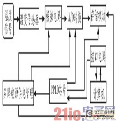
Figure 1 Schematic diagram of the temperature test system
2 Key technologies
2.1 Selection of main control chip CPLD
In this design, the XCR3128 produced by Xilinx is used as the main control CPLD chip of the temperature test system. XCR3128 has 100 pins, including 76 I/O pins, 4 signal interfaces, 4 global clocks, 7 VCCs, 8 GNDs, and 1 PORT_EN; it contains a total of 128 macro cells, VCC is 3.6 V, and the current limit is 200mA. XCR3128 has a small package and low power consumption, which fully meets the actual needs.
In this design, the control part is mainly composed of CPLD control circuit timing and working mode. The control function diagram is shown in Figure 2. The main functions are:
1) Power management and control module: This module mainly implements the power management and global clock control of the test system, thereby achieving the purpose of reducing power consumption and controlling the initial state of each signal.
2) Clock division module: This module mainly divides the clock output from the crystal oscillator to the CPLD, so as to obtain the timing required by the A/D converter, memory and FIFO.
3) Programming trigger comparison module: This module mainly realizes the programming of the trigger temperature digital level through a shift register; the digital comparison part compares the A/D conversion result with the programmed temperature digital level value to determine whether it is triggered or not.
4) FIFO and memory address module: This module mainly realizes the generation of addresses required by FIFO and memory, and the reading and writing of data of FIFO and memory.
5) A/D timing generation module: This module mainly implements the timing generation of the CONVST/ and read signals of the A/D converter.
6) Reading module: This module mainly implements the logical connection control of the reading interface and receives the pulse signal sent by the computer to complete the purpose of data transmission.
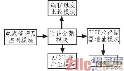
Figure 2 CPLD control function diagram of temperature test system
2.2 Temperature Sensor
In the harsh environment of high temperature, high pressure and high impact such as explosion field, the dynamic change of instantaneous temperature is very demanding for the temperature sensor, so the E12 tungsten-rhenium erosion thermocouple of NANMAC Company of the United States is selected. The transient temperature response time of this thermocouple is only a few hundred microseconds, the temperature range is up to 2315℃, and the pressure resistance is up to 69 MPa, which can fully meet the needs of explosion field temperature testing.
Thermocouples use the thermoelectric effect of conductors or semiconductor materials to convert temperature changes into changes in electromotive force. The electromotive force difference generated in the thermocouple circuit is:

NA and NB are the electron densities of materials A and B; σA and σB are the Thomson coefficients of conductors A and B, and K is the Boltzmann constant.
Since the electromotive force difference caused by the Thomson effect of the conductor is relatively small and can often be ignored, when the properties of the two materials of the thermocouple are known and the temperature of one end is fixed, the temperature to be measured T is a single-valued function of the electromotive force. In order to fix the cold end temperature of the E12 tungsten-rhenium thermocouple at 0°C, this design uses the compensation bridge method to compensate for the temperature change of the cold end.
2.3 Power Management Module
Since the temperature test system often needs to work in a harsh environment, the energy required is supplied by disposable high-temperature batteries, which have limited power. The temperature test system often requires a long test process. In order to reduce the possibility that the circuit cannot work properly due to insufficient power during the measurement process, the low power consumption requirement of the test system must be considered. Therefore, an advanced power management module is designed, that is, the circuit is powered when it needs to work, and the power is cut off when it does not need to work, reducing the proportion of power consumption when the circuit is ineffective.
In order to reduce unnecessary losses, a multi-power supply management mode is adopted, namely: VCC, VDD, VEE. VCC is connected to CPLD, the storage module part and AD conversion part are powered by VDD, and the operational amplifier and crystal oscillator are controlled by VEE.
In this system, the dual-channel power switch chip MAX894 is selected as the power management chip. Its power supply range is 2.7~5.5 V. When it is turned off, the current consumption is only 0.1μA. When both channels are turned on, the current consumption is about 17 μA. In this design, the input power supply VCC=3.6 V of the MAX894 chip is generated through ONA/control VDD=3.6 V, and through ONB/control VEE=3.6V. ONA/ONB/ is low level effective and is controlled by the CPLD. As shown in Figure 3. [page]

Figure 3 Temperature control system power management module
The control part of the power management module inside the CPLD is shown in Figure 4. ONON and OFF are switches of the circuit module, and TC/ is the enable terminal of the CPLD external crystal oscillator, which is valid at a high level. When the circuit is powered on, ONON becomes high, ONA becomes high, ONAN becomes low, the VDD output of the power management module is valid, and the AD conversion part and the storage module part start working. Since the crystal oscillator is in working state at this time, TC is low, ONBN is also low, and the VEE output of the power management part is valid. When the storage space of the memory is full, the crystal oscillator stops working, TC becomes high, and ONBN also becomes high, so the VEE output is invalid, and the operational amplifier part is turned off. At this time, the circuit is in a micro-power consumption state, and the memory is in a state of waiting for reading. When the data in the memory is read out, the circuit can be turned off. At this time, all devices except the CPLD are turned off.
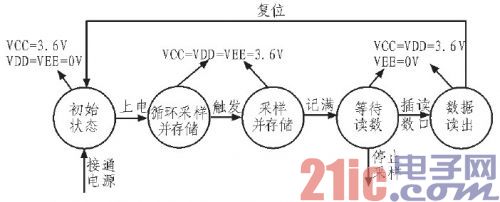
Figure 4 Power management module logic control diagram
3 Software Design
The workflow of the temperature test system is planned to be divided into five parts: the initial state of power on, the cyclic sampling state after power on, the sampling storage state after triggering, the waiting reading state after acquisition, the data reading and data processing state. The state transition diagram of the temperature test system is shown in Figure 5.

Figure 5 System state transition diagram
Figure 6 is a simulation timing diagram of the test system. Through multiple software simulations, correct simulation results are obtained, indicating that the temperature test system designed this time can meet the test requirements in theory.
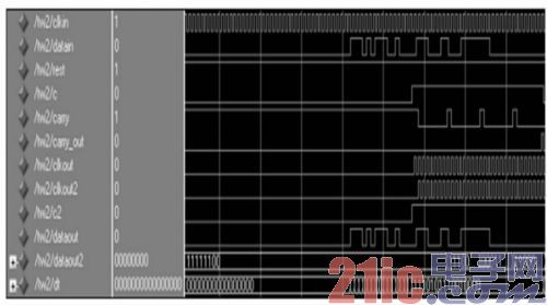
Figure 6 System timing simulation diagram
Figure 7 is the actual temperature test result diagram, which is obtained through VB software processing. In this experiment, the data curve collected by the temperature test system is basically consistent with the dynamic change of the given ambient temperature, indicating that the temperature test system based on CPLD designed this time can reliably and accurately collect data signals.
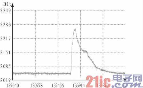
Figure 7 Measured data
4 Conclusion
The temperature test system designed this time adopts CPLD with high integration, strong reliability and low power consumption as the main control unit, and uses thermocouples with high temperature and high pressure resistance and fast response time as temperature sensors. It is matched with advanced power management modules to achieve low power consumption of the test system. Combined with dynamic storage test technology, it can be applied to harsh environments with poor environmental conditions, and can obtain better experimental data on the basis of reliability and micro power consumption.
Previous article:Pressure measurement in medical applications
Next article:Electromagnetic trigger controller based on CPLD
Recommended ReadingLatest update time:2024-11-16 16:03


- Popular Resources
- Popular amplifiers
-
 Learn CPLD and Verilog HDL programming technology from scratch_Let beginners easily learn CPLD system design technology through practical methods
 -
 Practical Electronic Components and Circuit Basics (4th Edition)_Explanation of basic circuit principles, introduction to electronic components, design of various circuits and practical circuit analysis
 -
 FPGA Principle and Structure (Zhao Qian)
 -
 EDA Technology Practical Tutorial--Verilog HDL Edition (Sixth Edition) (Pan Song, Huang Jiye)
- Keysight Technologies Helps Samsung Electronics Successfully Validate FiRa® 2.0 Safe Distance Measurement Test Case
- From probes to power supplies, Tektronix is leading the way in comprehensive innovation in power electronics testing
- Seizing the Opportunities in the Chinese Application Market: NI's Challenges and Answers
- Tektronix Launches Breakthrough Power Measurement Tools to Accelerate Innovation as Global Electrification Accelerates
- Not all oscilloscopes are created equal: Why ADCs and low noise floor matter
- Enable TekHSI high-speed interface function to accelerate the remote transmission of waveform data
- How to measure the quality of soft start thyristor
- How to use a multimeter to judge whether a soft starter is good or bad
- What are the advantages and disadvantages of non-contact temperature sensors?
- Innolux's intelligent steer-by-wire solution makes cars smarter and safer
- 8051 MCU - Parity Check
- How to efficiently balance the sensitivity of tactile sensing interfaces
- What should I do if the servo motor shakes? What causes the servo motor to shake quickly?
- 【Brushless Motor】Analysis of three-phase BLDC motor and sharing of two popular development boards
- Midea Industrial Technology's subsidiaries Clou Electronics and Hekang New Energy jointly appeared at the Munich Battery Energy Storage Exhibition and Solar Energy Exhibition
- Guoxin Sichen | Application of ferroelectric memory PB85RS2MC in power battery management, with a capacity of 2M
- Analysis of common faults of frequency converter
- In a head-on competition with Qualcomm, what kind of cockpit products has Intel come up with?
- Dalian Rongke's all-vanadium liquid flow battery energy storage equipment industrialization project has entered the sprint stage before production
- Allegro MicroSystems Introduces Advanced Magnetic and Inductive Position Sensing Solutions at Electronica 2024
- Car key in the left hand, liveness detection radar in the right hand, UWB is imperative for cars!
- After a decade of rapid development, domestic CIS has entered the market
- Aegis Dagger Battery + Thor EM-i Super Hybrid, Geely New Energy has thrown out two "king bombs"
- A brief discussion on functional safety - fault, error, and failure
- In the smart car 2.0 cycle, these core industry chains are facing major opportunities!
- The United States and Japan are developing new batteries. CATL faces challenges? How should China's new energy battery industry respond?
- Murata launches high-precision 6-axis inertial sensor for automobiles
- Ford patents pre-charge alarm to help save costs and respond to emergencies
- New real-time microcontroller system from Texas Instruments enables smarter processing in automotive and industrial applications
- DC-DC chip LM2596SX-5.0/NOPB
- How does the lwip client let the server know that it has been shut down?
- Small car front-end 16W power supply design
- TI's TPS61200 boost chip can only boost voltage but not reduce voltage during actual testing. Please help.
- Learn to make a flyback switching power supply-2
- Embedded Learning丨4412 Development Board-uboot Source Code-Assembly-Source Code Analysis (I)
- Using the I2C Bus
- 【Qinheng RISC-V core CH582】Learning material collection
- CCS cannot connect to F280049C Launchpad
- What topics do electronic engineers like?

 Learn CPLD and Verilog HDL programming technology from scratch_Let beginners easily learn CPLD system design technology through practical methods


 京公网安备 11010802033920号