Accurately measuring parasitic inductance is of great significance for the rational application of capacitors. This article introduces a method for measuring the parasitic inductance of capacitors using the LC resonance principle. A direct digital synthesizer is used to generate a programmable sweep signal to excite the capacitor containing parasitic inductance. At the same time, a logarithmic detector is used to detect the signal after passing through the network to be tested, and the DC signal output by the detector is collected using an AD converter. A specific program algorithm is used to compare the output levels of continuous frequency points, and finally the resonant point frequency is found to calculate the parasitic inductance of the capacitor itself. This solution uses a principle different from that of a conventional LCR bridge, so it is very suitable for measuring tiny inductors, and can accurately measure even tiny inductors used in the RF field. Its test results are very close to those tested using a network analyzer, and can basically meet most applications.
0 Introduction
Actual capacitor components have distributed parameters, among which parasitic inductance has the greatest impact on the characteristics of the capacitor itself. These parasitic inductances and the capacitor itself form a resonant circuit, which makes the capacitor have certain limitations when used. Therefore, being able to measure the size of the parasitic inductance of the capacitor itself can make it possible to choose capacitor components more reasonably when using it. Since the inductance of parasitic inductance is very small, mostly at the nH level, most LCR bridges cannot measure the parasitic inductance of the capacitor itself. In order to accurately measure parasitic inductance, this article describes a measurement method using the self-resonance principle. Combined with DDS sweep frequency technology, the parasitic inductance can be quickly measured. The measurement method is simple and accurate, and will be able to meet the application needs of most occasions.
1 Measurement Principle
Actual capacitors have parasitic inductance and parasitic resistance due to the manufacturing process. Its equivalent circuit model is shown in Figure 1.
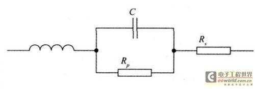
Figure 1 Actual capacitor equivalent circuit model
Where C is the nominal capacitance of the actual capacitor itself, L is its parasitic inductance, Rp is its parallel equivalent resistance, and Rs is its series equivalent resistance. Parasitic resistance will attenuate the signal passing through the capacitor, but will not affect the frequency characteristics of the capacitor itself. Parasitic inductance will form a series resonant circuit with the capacitor, causing the actual capacitor to resonate at a certain frequency. This phenomenon is called capacitor self-resonance. The impedance and frequency characteristic curve of the actual capacitor is shown in Figure 2.
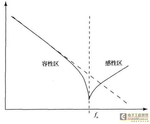
Figure 2 Actual capacitor frequency characteristic curve
f0 in Figure 2 is the resonant frequency of the resonant circuit composed of the capacitor and its parasitic inductance, which is called the self-resonant frequency. The solid line is the actual capacitor frequency characteristic curve, and the dotted line is the ideal capacitor characteristic curve without parasitic inductance. It can be seen that when the frequency is lower than the self-resonant frequency, the capacitor is capacitive, and the impedance decreases with the increase of frequency; however, when the frequency exceeds the self-resonant frequency, the capacitor shows a trend of increasing impedance with the increase of frequency, which is exactly the characteristic of inductance. The curve shows that the actual capacitor can only work below the self-resonant frequency. When it is higher than the self-resonant frequency, the capacitor is inductive and can no longer be used as a capacitor. It can be seen that accurately measuring the self-resonant frequency of the capacitor and finding its parasitic inductance are of great significance for the correct use of the capacitor. However, this inductance is often very small, usually at the nH level, and the general LCR bridge cannot measure this tiny inductance. Therefore, a method different from the bridge method is needed to measure this tiny inductance.
The resonant frequency of the LC series circuit composed of inductance and capacitance is:

At the same time, when resonance occurs, the impedance of the entire LC loop is purely resistive, that is, the sum of the inductive reactance and the capacitive reactance is zero. Using this principle, a sweep frequency signal is used to excite the capacitor to be tested, and the resonant frequency is measured. Then, combined with formula (1), the magnitude of the parasitic inductance can be measured. According to this principle, a sweep frequency generator is designed to generate a sweep frequency signal to excite the capacitor to be tested, and then the resonance point is found. The parasitic inductance of the capacitor can be calculated by reading the resonant frequency. Its structure is shown in Figure 3.
The most core parts are the sweep frequency generator and the resonance point detection circuit.
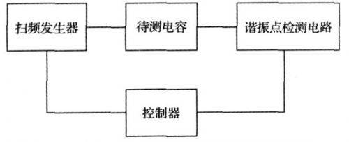
Figure 3 Parasitic inductance test device function [page]
2 Sweep frequency generator
The frequency sweep generator generates a wideband frequency sweep signal in this system to excite the capacitor to be tested. When the capacitance is large, take the common electrolytic capacitor as an example, assuming that the capacitance is 1000 F and its parasitic inductance is 100 nH, then according to formula (1), its self-resonant frequency can be calculated to be 15.9 kHz, which is a relatively low resonant frequency; take the ceramic capacitor as an example, assuming that its capacitance is 10 pF and its parasitic inductance is about 10 nH, then its self-resonant frequency is 500 MHz. The two signal frequencies differ by 4 orders of magnitude, which requires a wideband signal generator, which is also the design difficulty of this part. If the traditional analog signal generation method is used, in order to achieve the adjustable signal frequency, an LC oscillator composed of a varactor diode is generally used. However, when the signal frequency is low, the capacitance of the required varactor diode will be very large, and the capacitance value of the traditional varactor diode is generally only a few pF to several hundred pF, which is difficult to meet the low-frequency oscillation requirements. In order to simplify the frequency sweep circuit and realize digital control, DDS technology is used here to generate broadband signals. DDS uses the principle of DA converter, and realizes continuous waveform output through counter accumulation. The peripheral circuit of DDS chip is simple, and the signal frequency can be adjusted by writing its register. At the same time, the generated signal frequency resolution is high, generally reaching 0.01 Hz level, and the signal frequency span is large, which can realize continuous signals from a few Hz to hundreds of MHz, which is very suitable for sweep generator. Here, the AD9854 DDS chip is used. Under the drive of 300 MHz clock, it can generate a signal of up to 150 MHz according to the Nyquist sampling theorem. In order to obtain a better signal frequency, generally only a signal of up to 100 MHz is obtained. If you want to get a signal higher than 100 MHz, you can use its higher harmonics. The signal generation circuit based on AD9854 is shown in Figure 4. Due to space limitations, only the key output part and current setting part are drawn. AD9854 has a built-in 4~12 times clock multiplier, so a lower frequency clock can be added and multiplied to 300 MHz through the multiplier, which can greatly reduce the electromagnetic compatibility problems caused by the high-speed external clock to the system. AD9854 has a frequency control word register inside, and the frequency of the output signal can be changed by writing the value of this register, which is very suitable for digital control. At the same time, because the clock uses a crystal oscillator, the stability and resolution of the output frequency are very high, generally in the order of 10-6.
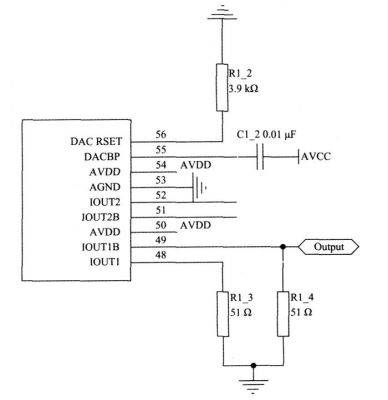
Figure 4 AD9854 signal generation circuit
3 Resonance point detection circuit
The resonance point detection circuit is mainly composed of a detector and an AD converter. Common detectors include peak detectors, effective value detectors, and logarithmic detectors. Since the detection here is only to detect the resonance point, there is no special requirement for the type of detector. Here, the AD8307 broadband logarithmic detector is used. AD8307 can realize a logarithmic detector within the DC 500 MHz frequency range. Its output is a DC voltage, and the output is linearly related to the input power (in dBm).
Since the detection circuit only detects the resonance point, that is, the lowest point in Figure 2, it is just a comparison relationship, and does not have high requirements for the level accuracy of the detected lowest point. Therefore, the accuracy requirements for the sampling circuit are not high. Because the output of the logarithmic detector is a DC signal, most common low-speed AD converters can meet the requirements. Here, the serial 8-bit AD converter TLC549 is used. TL549 adopts a three-wire serial control method, which is very convenient to interface with the single-chip controller. The schematic diagram of the detection circuit is shown in Figure 5.
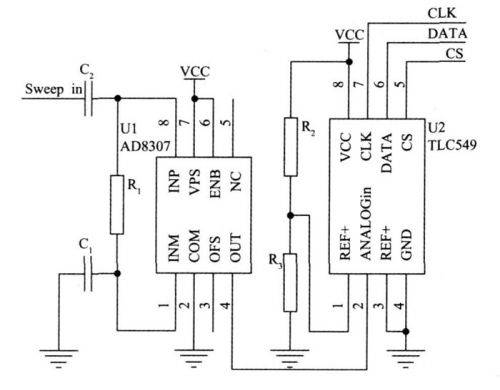
Figure 5 Resonance point detection circuit [page]
4 Main software process design
The single-chip microcomputer uses Atmeg16 to control the DDS and AD converter respectively, and is responsible for analyzing the calculation results. The single-chip microcomputer controls the DDS to output a signal each time, and collects the response result of this signal after passing through the circuit to be tested. This action is repeated three times and a comparison is performed. Because the level at the resonance point is the lowest, if the value of the middle one of the three collected data is the smallest, then this value is the level value at the resonance point. Record the frequency f at this time. Using formula (1), it can be known that:

Therefore, the L value can be obtained by equation (2). The flow chart of the main program is shown in Figure 6.
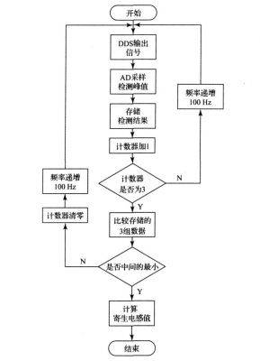
Figure 6 Main program flow
5 Experimental data analysis
A network analyzer is used to verify the test results of the designed tester.
The method of measuring parasitic inductance using a network analyzer is as follows: measure the forward transmission curve of the capacitor to be tested in parallel, obtain the curve shown in Figure 1, read the notch point frequency, and calculate the parasitic inductance value according to formula (1). Table 1 shows the comparison between the results of the parasitic inductance of capacitors of three orders of magnitude measured by the tester described in the article and the results measured by the network analyzer. The results shown in Table 1 are the final results after taking the average value of multiple measurements.
Table 1 Parasitic test results
It can be seen from Table 1 that for these three orders of magnitude of capacitors, the test result errors are all within 9%, which can basically meet the application requirements of most occasions.
Table 1 also shows that the measurement error increases as the capacitance value decreases. This phenomenon is caused by the low resolution of the swept frequency signal. Improving the resolution of the swept frequency signal can further reduce the error. In addition, the instrument cannot measure the parasitic inductance of capacitance less than 100 pF because the required excitation signal frequency exceeds the working range of AD9854. Using a higher frequency DDS can eliminate this problem.
6 Conclusion
The above scheme realizes the measurement of the parasitic inductance of the capacitor itself. Due to the DDS signal generation technology adopted, the frequency resolution is extremely high, which greatly improves the measurement accuracy of the inductance. This method can accurately measure the inductance of nH level, making up for the shortcoming that most LCR bridges cannot accurately measure tiny inductances. If this method is used in conjunction with the LCR bridge, it can basically meet the inductance measurement requirements in most cases.
Previous article:Introduction of Coordinate Measuring Machine
Next article:Discrimination terminal transistor tester
Recommended ReadingLatest update time:2024-11-16 18:06


- Popular Resources
- Popular amplifiers
- Keysight Technologies Helps Samsung Electronics Successfully Validate FiRa® 2.0 Safe Distance Measurement Test Case
- From probes to power supplies, Tektronix is leading the way in comprehensive innovation in power electronics testing
- Seizing the Opportunities in the Chinese Application Market: NI's Challenges and Answers
- Tektronix Launches Breakthrough Power Measurement Tools to Accelerate Innovation as Global Electrification Accelerates
- Not all oscilloscopes are created equal: Why ADCs and low noise floor matter
- Enable TekHSI high-speed interface function to accelerate the remote transmission of waveform data
- How to measure the quality of soft start thyristor
- How to use a multimeter to judge whether a soft starter is good or bad
- What are the advantages and disadvantages of non-contact temperature sensors?
- Innolux's intelligent steer-by-wire solution makes cars smarter and safer
- 8051 MCU - Parity Check
- How to efficiently balance the sensitivity of tactile sensing interfaces
- What should I do if the servo motor shakes? What causes the servo motor to shake quickly?
- 【Brushless Motor】Analysis of three-phase BLDC motor and sharing of two popular development boards
- Midea Industrial Technology's subsidiaries Clou Electronics and Hekang New Energy jointly appeared at the Munich Battery Energy Storage Exhibition and Solar Energy Exhibition
- Guoxin Sichen | Application of ferroelectric memory PB85RS2MC in power battery management, with a capacity of 2M
- Analysis of common faults of frequency converter
- In a head-on competition with Qualcomm, what kind of cockpit products has Intel come up with?
- Dalian Rongke's all-vanadium liquid flow battery energy storage equipment industrialization project has entered the sprint stage before production
- Allegro MicroSystems Introduces Advanced Magnetic and Inductive Position Sensing Solutions at Electronica 2024
- Car key in the left hand, liveness detection radar in the right hand, UWB is imperative for cars!
- After a decade of rapid development, domestic CIS has entered the market
- Aegis Dagger Battery + Thor EM-i Super Hybrid, Geely New Energy has thrown out two "king bombs"
- A brief discussion on functional safety - fault, error, and failure
- In the smart car 2.0 cycle, these core industry chains are facing major opportunities!
- The United States and Japan are developing new batteries. CATL faces challenges? How should China's new energy battery industry respond?
- Murata launches high-precision 6-axis inertial sensor for automobiles
- Ford patents pre-charge alarm to help save costs and respond to emergencies
- New real-time microcontroller system from Texas Instruments enables smarter processing in automotive and industrial applications
- [Anxinke NB-IoT Development Board EC-01F-Kit] V. Comprehensive Test
- 【Beetle ESP32-C3】VII. Network timing and weather request (Arduino)
- If anyone has a Concise Mechanical Manual, please send me a copy. I'd be very grateful.
- Here is the camera information on the national competition list
- 【Intelligent courtyard integrated control system】 Environmental parameter acquisition unit hardware
- One is okay, but two is not okay, so what about three?
- A collection of digital IC front-end design learning materials, one-click download without points
- RF Components Test Technology Seminar for 5G - You are invited to attend!
- What suitable domestic chips are recommended?
- Put down the textbook and look at the application circuit of the transistor

 MATLAB and FPGA implementation of wireless communication


 京公网安备 11010802033920号