Inventory of radio frequency interference rectification error circuits in amplifiers
Source: InternetPublisher:常思一二 Keywords: radio frequency interference amplifier rectification Updated: 2020/04/13
In real-world applications, an increasing amount of radio frequency interference (RFI) must be dealt with, especially where signal transmission lines are long and signal strength is low, as is the case with typical applications of instrumentation amplifiers due to their inherent common-mode rejection Ability to extract weaker differential signals from stronger common-mode noise and interference. But there is a potential problem that is often overlooked: RF rectification in instrumentation amplifiers . When strong RF interference is present, the integrated circuit may rectify the interference, which then manifests itself as a DC output offset error. Common-mode signals at the input of an instrumentation amplifier are usually attenuated by its common-mode rejection. RF rectification still occurs because even the best instrumentation amplifiers cannot actually reject common-mode noise at signal frequencies above 20 kHz. The amplifier's input stage may rectify strong RF signals, which then manifest themselves as DC offset errors. Once rectified, a low-pass filter at the instrumentation amplifier output will not be able to eliminate this error. If RFI is intermittent, it can cause undetectable measurement errors.
Designing Practical RFI Filters
The most practical solution to this problem is to use a differential low-pass filter before the instrumentation amplifier to attenuate the RF signal. This filter has three purposes: to remove as much RF energy from the input lines as possible; to balance the AC signals between each line and ground (common); and to maintain a high enough input impedance throughout the measurement bandwidth to Avoid loading the signal source.
Figure 1 is a basic block diagram of various differential RFI filters. The component values shown in the figure are all selected for the AD8221. The typical -3dB bandwidth value of the AD8221 is:
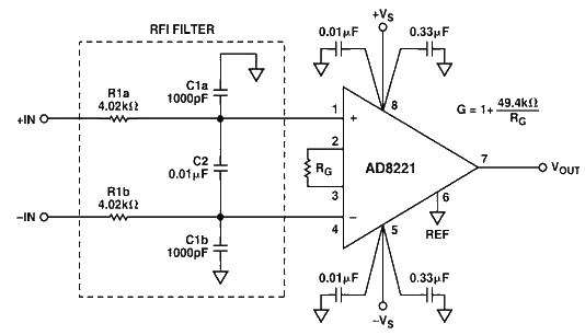
Figure 1 Low-pass filter circuit used to prevent radio frequency interference rectification errors
1MHz, typical voltage noise level is 7 nVQQ screenshot 20141204111321.jpg. In addition to suppressing radio frequency interference, this filter also has an input overload protection function. Because resistors R1a and R1b help isolate the instrumentation amplifier input circuit from external signal sources.
Figure 2 is a simplified diagram of this anti-RF interference circuit. As can be seen from the figure, the filter forms a bridge circuit with its output connected across the input pins of the instrumentation amplifier. Given this connection method, any mismatch between the two time constants of C1a/R1a and C1b/R1b will cause the bridge to be unbalanced, thereby reducing the high-frequency common-mode rejection performance. Therefore, resistors R1a and R1b and capacitors C1a and C1b should always be equal.
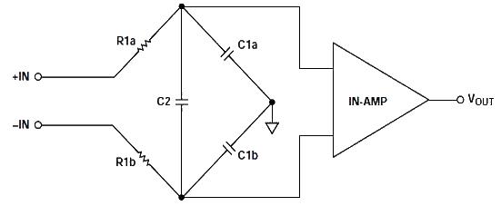
Figure 2 Capacitor C2 forms a bypass for C1a/C1b and can effectively reduce the AC common mode suppression error caused by component mismatch.
As shown in the figure, C2 is connected across the output of the bridge, so that C2 is actually in a parallel relationship with the series combination of C1a and C1b. When connected in this way, C2 can effectively reduce any AC common mode rejection error caused by mismatch. For example, if C2 is 10 times larger than C1, this connection will reduce the common-mode rejection error due to C1a/C1b mismatch to one-twentieth. It is important to note that this filter does not affect DC common mode rejection.
RFI suppression circuit for AD620 series instrumentation amplifiers
Figure 3 is a circuit for a general-purpose instrumentation amplifier (such as the AD620 series), which has a higher noise level (12 nVHz) and lower bandwidth than the AD8221 series. Accordingly, this type of instrumentation amplifier uses the same input resistor, but the value of capacitor C2 is increased approximately five times to 0.047 F to provide adequate RF attenuation. Using the values shown in the figure, the -3 dB bandwidth of the circuit is approximately 400Hz; by reducing the resistor values of R1 and R2 to 2.2 kΩ, the bandwidth can be increased to 760 Hz. It is important to note that the increased bandwidth comes at a cost , requiring the circuit in front of the instrumentation amplifier to drive a lower impedance load, thus reducing the input overload protection performance to a certain extent.
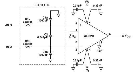
Figure 3 Radio frequency interference suppression circuit for AD620 series instrumentation amplifier
RFI Suppression Circuit for Micropower Instrumentation Amplifiers
Some instrumentation amplifiers are more susceptible to RF rectification than others , requiring stronger filters. A good example is a micropower instrumentation amplifier (such as the AD627) with low input stage operating current. The simple method of increasing the value of the two resistors R1a/R1b and/or the value of the capacitor C2 can improve the RF attenuation, but at the cost of reducing the signal bandwidth. Because the AD627 instrumentation amplifier has higher noise (38nV Hz) than general-purpose integrated circuits such as the AD620 family of devices, higher value input resistors can be used without significantly reducing the noise performance of the circuit. Figure 4 is a modification of the basic RC anti-RFI circuit shown in Figure 1 to use a higher value input resistor.
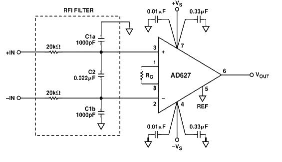
Figure 4 Radio frequency interference suppression circuit for AD627
The filter bandwidth is approximately 200 Hz. At a gain of 100 and an input of 1V pp, the maximum DC offset voltage is approximately 400 VRTI over the frequency range of 1 Hz to 20 MHz. When the gain remains unchanged, the circuit's RF signal suppression (output RF level/input RF level) will be better than 61 dB.
RFI Filter for AD623 Instrumentation Amplifier
Figure 5 shows an RFI immunity circuit recommended for use with the AD623 instrumentation amplifier. Since this device is less susceptible to radio frequency interference than the AD627, the value of the input resistor can be reduced from 20 kΩ to 10 kΩ. This will increase the signal bandwidth of the circuit and reduce the resistor's noise contribution. Additionally, the 10k resistor provides extremely effective input protection. When using the values shown in the figure, the bandwidth of the filter is about 400Hz. When the gain is 100 and the input is 1Vp-p, the maximum DC offset voltage is less than 1 V RTI. When the gain is unchanged, the RF signal suppression of the circuit is better than 74 dB. [!--empirenews.page--]
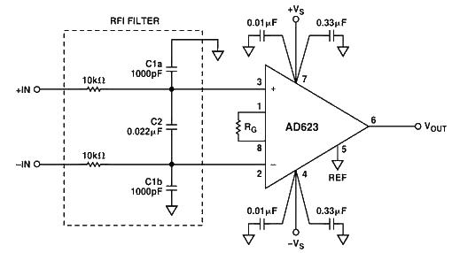
Figure 5 AD623 radio frequency interference suppression circuit
AD8225 radio frequency interference filter circuit
Figure 6 shows the recommended RFI filter for this instrumentation amplifier. The AD8225 instrumentation amplifier has a fixed gain of 5 and is more susceptible to radio frequency interference than the AD8221. Without an RFI filter, the measured DC offset voltage of this instrumentation amplifier is approximately 16 mV RTI when inputting a 2 Vp-p, 10 Hz to 19 MHz sine wave. This filter achieves higher RF attenuation than the AD8221 circuit by using larger value resistors: 10 kΩ instead of 4 kΩ. This is acceptable due to the higher noise level of the AD8225. If a filter is used, the DC offset voltage error is negligible.
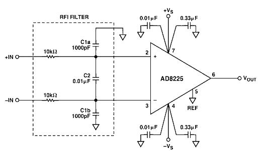
Figure 6 AD8225 radio frequency interference filter circuit
Using common-mode RF chokes as instrumentation amplifier RF interference filters
As an alternative to the RC input filter, a commercial common-mode RF choke can be connected in front of the instrumentation amplifier, as shown in Figure 7. A common mode choke is a dual-winding RF choke that uses a common core. Any common-mode input RF signal at both inputs will be attenuated by the choke. Common mode chokes provide a simple way to suppress radio frequency interference with a small number of components while achieving a wider signal passband, but the effectiveness of this method depends on the quality of the common mode choke used, and it is best to use Well matched internal choke. Another potential problem with using a choke is that it does not provide the same level of input protection as an RC RFI filter. Using an AD620 instrumentation amplifier with an RF choke and a rated gain of 1000, the circuit shown in Figure 7 can reduce the DC offset voltage to less than 4.5 V RTI when inputting a 1 Vp-p common-mode sine wave. The high-frequency common-mode rejection ratio is also significantly reduced, as shown in Table I.
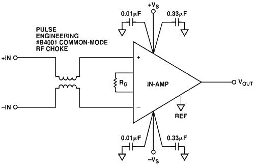
Figure 7 Using a commercial common-mode RF choke to suppress RF interference
Because some instrumentation amplifiers are more susceptible to RF interference than others, using a common-mode choke is sometimes not enough to solve the problem. In these cases it is better to use an RC input filter.
Radio frequency interference test
Figure 8 shows a typical setup for RFI suppression testing. To test the RFI rejection of these circuits , connect the two inputs with very short leads. Connect a high-quality sine wave generator to this input with a 50-gauge terminated cable.
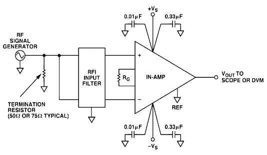
Figure 8 Typical setup for instrumentation amplifier RFI suppression measurements
Get an oscilloscope and adjust the sine wave generator so that the output at the generator end is 1 V pp. Set the instrumentation amplifier to high gain (such as 100). The DC offset voltage can be read directly at the output of the instrumentation amplifier with a digital voltmeter (DVM). To measure high-frequency common-mode rejection, connect an oscilloscope to the instrumentation amplifier output through a compensated probe and measure the peak-to-peak output voltage (ie, feedthrough) with respect to the input frequency. When calculating common-mode rejection ratio over frequency, be sure to consider the input termination (VIN/2) and the instrumentation amplifier gain.
- TPS274C65 helps reduce downtime and increase productivity in 24 VDC power distribution plants
- Energy-saving motorcycle rectifier regulator
- Driving circuit that controls LED brightness using PWM signal
- LED rechargeable flashlight circuit diagram
- Principles and precautions of active discharge circuit
- LNK304 non-isolated LED light string driver circuit
- A small and easy-to-make fast charger
- Power supply circuit that can reduce LM317 ripple
- Homemade low-power UPS
- CNC regulated power supply production
- High performance broadband GaN power amplifier
- Heart rate detection circuit
- Two-channel audio power amplifier circuit diagram analysis
- Sense amplifier circuit
- Inductively Coupled Voltage Amplifier Circuit
- MC-1590 IF amplifier circuit diagram
- High input impedance three op amp differential amplifier circuit diagram
- High input impedance three op amp differential amplifier circuit diagram
- LTC2053 thermocouple amplification circuit diagram
- Basic Op Amp Differential Amplifier


 京公网安备 11010802033920号