Home >
Basic Circuits >Silicon Controlled Phase > The working principle and basic characteristic circuit of silicon controlled components
The working principle and basic characteristic circuit of silicon controlled components
Source: InternetPublisher:赔钱虎 Updated: 2012/12/25
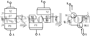
The thyristor is a P1N1P2N2 four-layer three-terminal structural component with a total of three PN junctions. When analyzing the principle, it can be regarded as consisting of a PNP tube and an NPN tube. Its equivalent diagram is shown in Figure 1. Figure
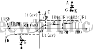
 1 Silicon-controlled equivalent diagram: When forward voltage is applied to anode A, both BG1 and BG2 tubes are in an amplified state. At this time, if a positive trigger signal is input from the control electrode G, BG2 will have base current ib2 flowing through it. After being amplified by BG2, its collector current ic2 = β2ib2. Because the collector of BG2 is directly connected to the base of BG1, ib1=ic2. At this time, the current ic2 is amplified by BG1, so the collector current of BG1 is ic1=β1ib1=β1β2ib2. This current flows back to the base of BG2, forming a positive feedback, causing ib2 to continuously increase. As a result of this forward feed cycle, the current of the two tubes increases sharply, and the thyristor becomes saturated and conducts. Due to the positive feedback effect formed by BG1 and BG2, once the thyristor is turned on, even if the current of the control electrode G disappears, the thyristor can still maintain the on state, because the trigger signal only acts as a trigger and does not turn off. function, so this thyristor cannot be turned off. Since the thyristor has only two working states: on and off, it has switching characteristics. This characteristic requires certain conditions to be transformed. This condition is shown in Table 1. Table 1 Description of the conditions for the thyristor to be turned on and off. From turn-off to turn-on 1. The anode potential is higher than the cathode potential 2. The control electrode has sufficient forward voltage and current, both of which are indispensable to maintain conduction 1. The anode potential is higher than the cathode potential 2. The anode current is greater than the maintaining current Either one is indispensable from turn-on to turn-off 1. The anode potential is lower than the cathode potential 2. The anode current is less than the holding current, any condition is sufficient 2. Basic volt-ampere characteristics The basic volt-ampere characteristics of the thyristor are shown in Figure 2
 Figure 2 Basic volt-ampere characteristics of silicon control (1) Reverse characteristics When the control electrode is open and reverse voltage is applied to the anode (see Figure 3), the J2 junction is forward biased, but the J1 and J2 junctions are reverse biased. At this time, only a small reverse saturation current can flow. When the voltage further increases to the avalanche breakdown voltage of the J1 junction, the junction J3 also breaks down, the current increases rapidly, and the characteristics in Figure 3 begin to bend, such as the characteristic OR As shown in the paragraph, the voltage URO at the bend is called "reverse turning voltage". At this time, the thyristor will undergo permanent reverse breakdown.
 Figure 3 Reverse voltage applied to the anode (2) Forward characteristics When the control electrode is open circuit and forward voltage is applied to the anode (see Figure 4), the J1 and J3 junctions are forward biased, but the J2 junction is reverse biased, which is different from the ordinary PN junction. The reverse characteristics are similar, and only a small current can flow. This is called the forward blocking state. When the voltage increases, the characteristics in Figure 3 are bent, as shown in the characteristic section OA. The bend is UBO, which is called: forward Turning voltage
 Figure 4: When forward voltage is applied to the anode, after the voltage rises to the avalanche breakdown voltage of the J2 junction, the avalanche multiplication effect occurs at the J2 junction, generating a large number of electrons and holes in the junction area. The electrons enter the N1 area and the holes When entering the P2 area. The electrons entering the N1 region recombine with the holes injected into the N1 region from the P1 region through the J1 junction. Similarly, the holes entering the P2 region recombine with the electrons injected into the P2 region from the N2 region through the J3 junction, causing avalanche breakdown. The electrons and holes entering the P2 region cannot all recombine. In this way, electrons accumulate in the N1 region and holes accumulate in the P2 region. As a result, the potential of the P2 region increases, the potential of the N1 region decreases, and the J2 junction It becomes forward biased. As long as the current increases slightly, the voltage will drop rapidly and the so-called negative resistance characteristic will appear. See the dotted line AB in Figure 3. At this time, the three junctions J1, J2, and J3 are all in forward bias, and the thyristor enters the forward conducting state---on state. At this time, its characteristics are similar to the forward characteristics of ordinary PN junctions, as shown in Figure 2 BC segment 3. Trigger conduction When a forward voltage is added to the control electrode G (see Figure 5), due to the forward bias of J3, holes in the P2 area enter the N2 area, and electrons in the N2 area enter the P2 area, forming a trigger current IGT. . On the basis of the internal positive feedback effect of the thyristor (see Figure 2), coupled with the effect of the IGT, the thyristor is turned on in advance, causing the OA segment of the volt-ampere characteristics in Figure 3 to shift to the left. The larger the IGT, the left Move faster.
 Figure 5 Positive voltage is applied to both the anode and the control electrode
 1 Silicon-controlled equivalent diagram: When forward voltage is applied to anode A, both BG1 and BG2 tubes are in an amplified state. At this time, if a positive trigger signal is input from the control electrode G, BG2 will have base current ib2 flowing through it. After being amplified by BG2, its collector current ic2 = β2ib2. Because the collector of BG2 is directly connected to the base of BG1, ib1=ic2. At this time, the current ic2 is amplified by BG1, so the collector current of BG1 is ic1=β1ib1=β1β2ib2. This current flows back to the base of BG2, forming a positive feedback, causing ib2 to continuously increase. As a result of this forward feed cycle, the current of the two tubes increases sharply, and the thyristor becomes saturated and conducts. Due to the positive feedback effect formed by BG1 and BG2, once the thyristor is turned on, even if the current of the control electrode G disappears, the thyristor can still maintain the on state, because the trigger signal only acts as a trigger and does not turn off. function, so this thyristor cannot be turned off. Since the thyristor has only two working states: on and off, it has switching characteristics. This characteristic requires certain conditions to be transformed. This condition is shown in Table 1. Table 1 Description of the conditions for the thyristor to be turned on and off. From turn-off to turn-on 1. The anode potential is higher than the cathode potential 2. The control electrode has sufficient forward voltage and current, both of which are indispensable to maintain conduction 1. The anode potential is higher than the cathode potential 2. The anode current is greater than the maintaining current Either one is indispensable from turn-on to turn-off 1. The anode potential is lower than the cathode potential 2. The anode current is less than the holding current, any condition is sufficient 2. Basic volt-ampere characteristics The basic volt-ampere characteristics of the thyristor are shown in Figure 2
 Figure 2 Basic volt-ampere characteristics of silicon control (1) Reverse characteristics When the control electrode is open and reverse voltage is applied to the anode (see Figure 3), the J2 junction is forward biased, but the J1 and J2 junctions are reverse biased. At this time, only a small reverse saturation current can flow. When the voltage further increases to the avalanche breakdown voltage of the J1 junction, the junction J3 also breaks down, the current increases rapidly, and the characteristics in Figure 3 begin to bend, such as the characteristic OR As shown in the paragraph, the voltage URO at the bend is called "reverse turning voltage". At this time, the thyristor will undergo permanent reverse breakdown.
 Figure 3 Reverse voltage applied to the anode (2) Forward characteristics When the control electrode is open circuit and forward voltage is applied to the anode (see Figure 4), the J1 and J3 junctions are forward biased, but the J2 junction is reverse biased, which is different from the ordinary PN junction. The reverse characteristics are similar, and only a small current can flow. This is called the forward blocking state. When the voltage increases, the characteristics in Figure 3 are bent, as shown in the characteristic section OA. The bend is UBO, which is called: forward Turning voltage
 Figure 4: When forward voltage is applied to the anode, after the voltage rises to the avalanche breakdown voltage of the J2 junction, the avalanche multiplication effect occurs at the J2 junction, generating a large number of electrons and holes in the junction area. The electrons enter the N1 area and the holes When entering the P2 area. The electrons entering the N1 region recombine with the holes injected into the N1 region from the P1 region through the J1 junction. Similarly, the holes entering the P2 region recombine with the electrons injected into the P2 region from the N2 region through the J3 junction, causing avalanche breakdown. The electrons and holes entering the P2 region cannot all recombine. In this way, electrons accumulate in the N1 region and holes accumulate in the P2 region. As a result, the potential of the P2 region increases, the potential of the N1 region decreases, and the J2 junction It becomes forward biased. As long as the current increases slightly, the voltage will drop rapidly and the so-called negative resistance characteristic will appear. See the dotted line AB in Figure 3. At this time, the three junctions J1, J2, and J3 are all in forward bias, and the thyristor enters the forward conducting state---on state. At this time, its characteristics are similar to the forward characteristics of ordinary PN junctions, as shown in Figure 2 BC segment 3. Trigger conduction When a forward voltage is added to the control electrode G (see Figure 5), due to the forward bias of J3, holes in the P2 area enter the N2 area, and electrons in the N2 area enter the P2 area, forming a trigger current IGT. . On the basis of the internal positive feedback effect of the thyristor (see Figure 2), coupled with the effect of the IGT, the thyristor is turned on in advance, causing the OA segment of the volt-ampere characteristics in Figure 3 to shift to the left. The larger the IGT, the left Move faster.
 Figure 5 Positive voltage is applied to both the anode and the control electrode
 Latest Basic Circuits Circuits
- Analysis of the working principle of CMOS/CCD image sensor
- What are the types of commonly used batteries?
- Working principle/characteristics/application fields/equivalent circuit of unijunction transistor
- How does RCCB work?
- Why use PWM? What are its advantages?
- What types of force sensors are there?
- FL52C4 induction electronic greeter
- Using Monostable Trigger to Construct Pulse Delay Circuit
- Odd-frequency counter with symmetrical output waveform (SN7474, SN74163)
- An easy-to-make counting frequency meter
Popular Circuits
- 555 square wave oscillation circuit
- 555 photo exposure timer circuit diagram
- Introducing the CD4013 washing machine timer circuit diagram
- Simple level conversion circuit diagram
- 555 electronic guide speaker circuit diagram for blind people
- Circuit diagram of disconnection alarm composed of 555
- Analog circuit corrector circuit diagram
- color discrimination circuit
- Color sensor amplification circuit
- Level indication circuit


 京公网安备 11010802033920号