5 Converter Topologies for Integrated Solar and Storage Systems
Source: InternetPublisher:newlandmark Keywords: Solar energy Energy storage system Converter topology Updated: 2025/01/16
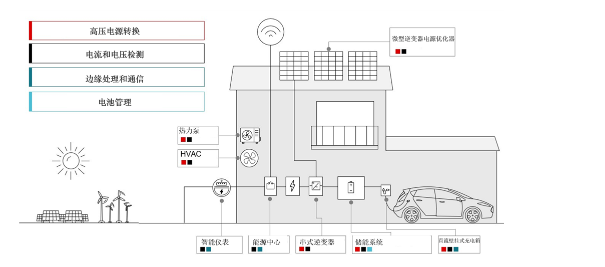
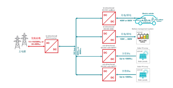
Energy storage systems are becoming more affordable and electricity prices are rising, so the demand for renewable energy is increasing. Many homes now use a combination of solar generation and battery storage to ensure energy is available when solar power cannot meet demand. Figure 1 shows a residential use case, and Figure 2 shows how a typical PV inverter system can be integrated with an energy storage system.

Figure 1: A residential solar power generation and energy storage system installation scheme

Figure 2: Typical PV inverter system with energy storage system
Ideally, this type of system has efficient power management components that enable AC/DC and DC/DC conversion and high power density (with the smallest possible solution size), which are highly reliable (ultra-low losses) and help bring products to market quickly. However, these requirements are not always possible at the same time, and trade-offs need to be made regarding the ideal power conversion topology for these sub-blocks.
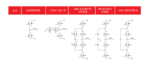
Common to existing power topologies for AC/DC and DC/DC buck and boost power converters is the interleaved operation of half-bridges or converter branches, designed to increase power levels in DC/DC converters or to achieve three-phase operation in AC/DC inverters or power factor correction stages by placing three branches running at 120 degrees phase shift. Figure 3 shows a simplified schematic of five power topologies.

Figure 3: Half-bridge power supply topology and equivalent branched power supply topology
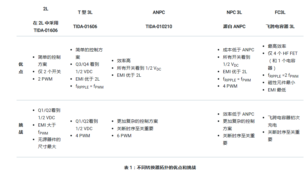
Topology 1: In a two-stage converter topology, pulse width modulation (PWM) signals are applied to power devices Q1 and Q2 as complementary (with time delay to avoid shoot-through due to overlapping switching signals). For a positive sine wave at the output, Q1 is applied with a duty cycle of >50%. For a negative sine wave at the output, Q2 is applied with a duty cycle of >50%. Controlling the output power is a simple concept, but the output signal before the line filter has a full bus voltage swing, which requires a larger filter to reduce EMI. The ripple frequency entering the filter is the PWM frequency, which affects the filter size.
Compared to a two-stage converter, a three-level topology allows for the use of smaller passive components and has lower EMI. There are four three-level topologies:
Topology 2: The T-type topology gets its name from the way the transistors are arranged around the neutral point (VN). Q1 and Q2 are connected to the DC link, while Q3 and Q4 are in series with VN. The ripple frequency seen by the filter is equal to the PWM frequency applied to switches Q1 to Q4. This determines how large the filter components need to be to achieve the desired low total harmonic distortion at the AC line frequency. Q1 and Q2 see the full bus voltage, which needs to be rated at 1,200V when the DC link voltage in the system is 800V. Since Q3 and Q4 are connected to VN, they only see half of the full bus voltage, and in an 800-V DC link voltage system, they are rated at 600V, which can save on converter type costs. Learn about the 10kW bidirectional three-phase three-level (T-type) inverter and PFC reference design.
拓扑 3:在有源中性点箝制 (ANPC) 转换器拓扑结构中,VN 与有源开关 Q5 和 Q6 连接,并将 VN 设置在直流链路电压的中间。与 T 型转换器一样,滤波器看到的纹波频率等于用来确定交流线路滤波器尺寸的 PWM 频率。这种架构的优点是所有开关的额定电压都是最大直流链路电压的一半;在 800V 系统中,可以使用额定电压为 600V 的开关,因此有助于节省成本。关闭此转换器时,务必将每个开关上的所有电压限制为直流链路电压的一半。换句话说,控制微控制器 (MCU) 需要处理关断时序。TI 的 TMS320F280049C 和 C2000TM 产品系列中的其他器件具有可配置的逻辑,允许在硬件中实现关机逻辑,以卸下 MCU 的软件任务。了解基于 GaN 的 11kW 双向三相 ANPC 参考设计。
拓扑 4:中性点箝制 (NPC) 转换器拓扑结构来自 ANPC 拓扑结构。这里的 VN 通过二极管 D5 和 D6 连接,将 VN 设置在直流链路电压中间。 滤波器看到的输出纹波频率等于用来确定交流线路滤波器尺寸的 PWM 频率。与 ANPC 拓扑一样,所有开关的额定电压都是最大直流链路电压的一半,但有另外两个开关需改为两个快速二极管。与 ANPC 拓扑相比,NPC 拓扑的成本略有降低,但代价是效率也略有降低。关断时序的要求也与 ANPC 拓扑相同。从上述 ANPC 参考设计中很容易推导出 NPC 拓扑。
Topology 5: Flying Capacitor Topology You already know what happens in this converter; a capacitor is connected to the switch nodes of the stacked half-bridge implemented by Q1 and Q2, and Q3 and Q4. The voltage across the capacitor is limited to half the DC link voltage and drifts periodically between V+/V–; power delivery occurs during this drift. This topology uses all switches during both the positive and negative sine waves. In this topology, the output ripple frequency seen by the filter is twice the PWM frequency provided by the flying capacitor drifting each cycle, so the size of the AC line filter is smaller. Also, all switches are rated for half the maximum DC link voltage, which helps save cost

All four three-level topologies offer clear advantages over conventional two-level converters in terms of power density (with the smallest possible solution size), highly reliable operation, and fast time to market. These advantages are further enhanced by the use of wide bandgap devices and high-performance MCUs at reasonable costs.
- How to Make a Soft Latch Circuit
- Driving circuit of switching power supply field effect tube
- Offline 8w LED Flyback Power Supply with PFC using NCP1014
- Charging control circuit made by solar energy
- CNC regulated power supply production
- Design of electric vehicle charger
- UC3842 Electric Vehicle Charger
- Adjustable voltage regulated power supply circuit
- Homemade Electric Bike Fast Charger
- LM317T voltage regulation adjustable circuit diagram explanation
- Single solar battery charger working circuit
- Solar flasher principle circuit
- Novel solar LED light controller circuit diagram
- Solar lawn light circuit
- Voltage stabilization control circuit in power circuit
- 2-phase CPU power supply circuit using HIP6302 and HIP6602 chips
- Low voltage adjustable reference power circuit
- Solar flashlight supercapacitor storage circuit
- Industrial four-way programmable controller power circuit
- Hefei Sunshine Solar and Wind Power SD Intelligent Controller


 京公网安备 11010802033920号