|
The OP
Published on 2023-12-12 22:03
Only look at the author
This post is from PCB Design
| ||
|
Personal signature
射频【放大器】 |
||
This post is from PCB Design
| ||
|
Personal signature
射频【放大器】 |
||
|
|
This post is from PCB Design
| ||
|
Personal signature
射频【放大器】 |
||
|
|
This post is from PCB Design
| ||
|
Personal signature
射频【放大器】 |
||
|
|
This post is from PCB Design
| ||
|
Personal signature
射频【放大器】 |
||
|
|
This post is from PCB Design
| ||
|
Personal signature
射频【放大器】 |
||
|
|
This post is from PCB Design
| ||
|
Personal signature
射频【放大器】 |
||
|
|
- 【Posts】Surface roughness of copper foil of 5G printed circuit board
- 【Posts】Surface Roughness Compensation, Gradient, and Other Methods Application Note AP8206
- 【Posts】Usage and application scenarios of 5G wireless comprehensive tester
- 【Posts】MWC 2024: Intel promotes the transformation and upgrading of network infrastructure with green 5G core network chips
- 【Posts】Reply and give points: 5G is coming, will you change to a 5G mobile phone?
- 【Posts】Zhang Chaoyang questioned 5G: Such high-frequency electromagnetic waves are very harmful to the human body
- 【Posts】Have you used 5G? 6G is coming
- 【Posts】Ride: Which country will be the ultimate winner in 5G? Reply to this post and give points
- 【Download】Optimization research on low-power power system design based on 5G communication technology
- 【Download】Research on power supply and distribution technology for 5G communication base stations_Gou Zengjie
- 【Download】High-speed rail 5G antenna technology and selection application analysis
- 【Download】5G and Internet of Vehicles - Internet of Vehicles technology and intelligent connected cars based on mobile communications
- 【Download】Interpretation of 5G New Radio -- Latest Developments in 3GPP and ITU Standards
- 【Download】ARM White Paper: The Road to 5G: Key Features and Technologies Required for Next-Generation Cellular Communications
- 【Download】NI 5G Semiconductor Test Engineer\'s Guide
- 【Download】The Way of Communication - From Calculus to 5G
- 【Design】Open source DIY: WiFi, 4G, 5G remote control drones/unmanned ships, image transmission/data transmission/remote control integration!
- 【Design】USB3.0 ultra-short male patch PCB board. For use in MAC PRO A1289 and G5 chassis modification.
- 【Design】USB3.0 ultra-short male patch PCB board. For use in MAC PRO A1289 and G5 chassis modification.
- 【Design】SECO-NCP51561BADWR2G-GEVB: Application daughter card for NCP51561 5 kV isolated half-bridge gate driver
- 【Design】5G28 operational amplifier
- 【Design】5G23 operational amplifier
- 【Circuits】How to protect 5G macro base station amplifiers and antennas from electrical hazards
- 【Circuits】The German government confirms that Huawei will not be excluded from 5G network construction
- 【Circuits】5G RF front-end module, do you understand it?
- 【Circuits】Type ADXL05 monolithic acceleration sensor circuit with signal conditioning ±1g to ±5g
- 【Circuits】Recommendations for 5G small base station power supply design
- 【Circuits】RF FUSION? 5G Chipset
- 【Articles】Strong market demand for 5G base stations/consumer electronics and other markets leads to an increase in both volume and price of PCB/copper clad laminates
- 【Articles】5G network speed is faster than 4G, but the perception is poor! Wu Hequan: 6G standard formulation should focus on user needs
- 【Articles】Upgrading automotive signal management with 5G to prepare for the future
- 【Articles】MeiG Intelligent 5G Automotive-Grade Communication Module: 5G+C-V2X Connects Automotive Communications for the Next Decade
- 【Articles】Picotech's Surge China Chip Enables the First Nationally Produced 5G Wireless Cloud Network and Mobile Communication Service Innovation
- 【Articles】Yu Chengdong: ADS 3.0 is not L3 yet. Hongmeng Zhixing's OTA is upgraded through 5G technology
-
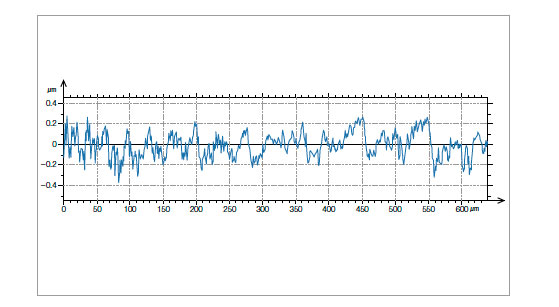
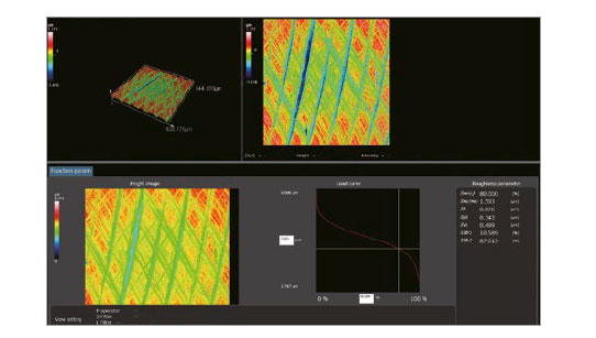
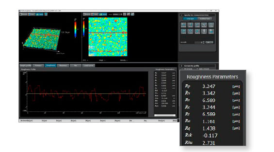
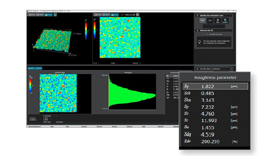
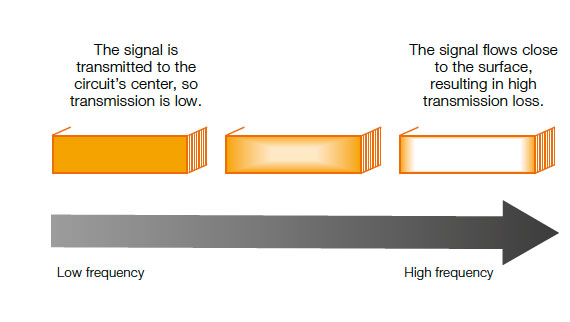
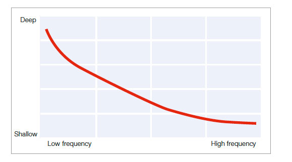
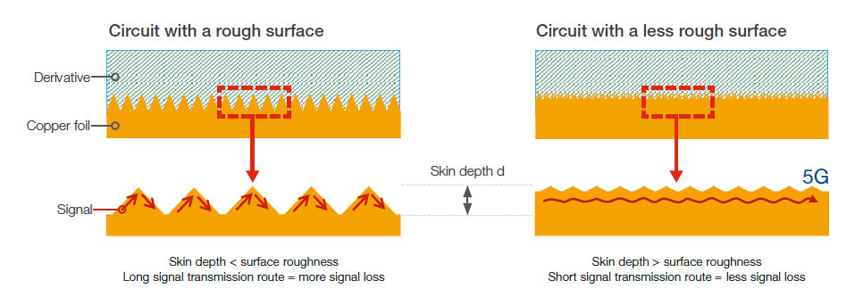
Surface roughness of copper foil of 5G printed circuit board
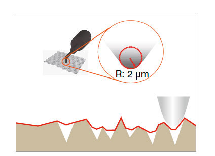
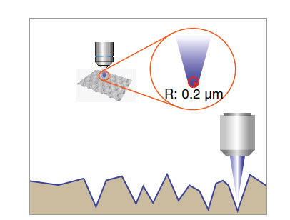
MeasuringRoughnessBeyondRz(MaximumHeight)UsingLaserMicroscopeAnalyzingSurfaceRoughnessofCopperFoilon5GPrintedCircuitBoardsTherapidspreadofmobilephoneshasdriveninnovationinmobilecommunicationsystems,whichundergomajortechnologicalchangesappro ...
-
Surface Roughness Compensation, Gradient, and Other Methods Application Note AP8206
ChoosingtheRightSurfaceRoughnessMeasurementTherearemanysurfaceroughnesscompensationmodelsthatcanhelpdesignersandmanufacturerssimulatetheeffectsofcopperroughnessoninsertionlossHuray(Canonball)acceptsRzorSEMdataifavailable,andGradientacceptsR ...
-
Wireless Charging Foreign Object Detection FOD
WirelessChargingForeignObjectDetectionFOD
- Download data page shows dx
- How to convert the copper foil of the package substrate into a pad, or directly add a pin number
- Transfer of a number of idle personal 100M digital oscilloscope signal generators
- 【ATmega4809 Curiosity Nano Review】Timer
- How to retrieve the component library that comes with AD software if it is missing?
- CPU reads and writes memory
- TI C2000 LaunchPad uses official routines to compile and debug
EEWorld Datasheet Technical Support
-
Huawei's Strategic Department Director Gai Gang: The cumulative installed base of open source Euler operating system exceeds 10 million sets
On November 15, it was reported that the first AI native open source operating system of openEule
-
Whether it is the electrification of automobiles or generative artificial intelligence, power tec
-
Wi-Fi 8 specification is on the way: 2.4/5/6GHz triple-band operation
MediaTek has released a white paper on its official website, outlining some details of the next-g
- Vietnam's chip packaging and testing business is growing, and supply-side fragmentation is splitting the market
- Apple faces class action lawsuit from 40 million UK iCloud users, faces $27.6 billion in claims
- The US asked TSMC to restrict the export of high-end chips, and the Ministry of Commerce responded
- ASML predicts that its revenue in 2030 will exceed 457 billion yuan! Gross profit margin 56-60%
- Qualcomm launches its first RISC-V architecture programmable connectivity module QCC74xM, supporting Wi-Fi 6 and other protocols
- It is reported that memory manufacturers are considering using flux-free bonding for HBM4 to further reduce the gap between layers
- ON Semiconductor CEO Appears at Munich Electronica Show and Launches Treo Platform
- Problems with STM32 and passive buzzer playing sound
- Embedded Tutorial_DSP Technology_DSP Experiment Box Operation Tutorial: 2-28 Building a Lightweight WEB Server Experiment
- OPA847IDBVR op amp domestic replacement
- AG32VF407 Test UART
- [Digi-Key Follow Me Issue 2] Chapter 1: Sharing on receiving the goods
- What model is this infrared receiver? Which model can be used instead? Thank you
- Selling brand new unopened ZYNQ 7Z020 FPGA core board
- The LORA module used in the lithium battery-powered water meter setting can save energy when 100 water meters are installed in one corridor.
- I would like to ask, when a port is set to RX0, is it necessary to set the input and output direction of this port?
- Why is this year so difficult? It’s even more difficult than during the pandemic. I’m 30 and facing unemployment. I’m so confused.
- Ask about the voltage regulator test question
- [Xiaohua HC32F448 Review] About Xiaohua Semiconductor's UART interrupt sending and PRINTF construction and redirection
- 【BIGTREETECH PI development board】 HDMI output test
- 【BIGTREETECH PI development board】+08. Audio test (zmj)
- [Xiaohua HC32F448 Review] +RTC electronic clock
- Embedded Engineer AI Challenge Camp (Advanced): Deploy InsightFace algorithm on RV1106 for real-time face recognition of multiple people
- # STM32H7S78-DK Development Kit Three-week Review: Implementation and Analysis of Simple Sound Collection and Storage Using SD Card Reading and Writing
- [STM32H7R/S] Review⑧ nano edge ai studio training a model--Part 1
- [2024 DigiKey Creative Competition] A "fortune-telling" artifact based on Raspberry Pi
- New energy vehicle on-board AC slow charging and maintenance
- Embedded Engineer AI Challenge Camp (Advanced): Deploy InsightFace algorithm on RV1106 for real-time face recognition of multiple people
- I want to make a self-driving car. I saw one on Bilibili that costs 300 yuan. I am hesitant.
- [K230 Embedded AI Development Board Review] + License Plate Recognition and Billing Management
- How to deploy LVGL free graphics library on low-cost ARM platform, based on Allwinner T113-i
- Please help me analyze the reasons why EMI fails.
- 参会有好礼 | 2024 瑞萨电子MCU/MPU工业技术研讨会
- 深圳站:11月30日(周六)深圳湾万怡酒店
上海站:12月06日(周五)上海喜玛拉雅酒店
奖励设置:现金红包、螺丝刀套装或30元京东卡
- Littelfuse 新品赋能电子产品安全可靠并高效, 10+挑战等你探索!
- Littelfuse 应用赋能星球,覆盖了诸多应用痛点及解决办法,邀请工程师一起探索,解锁更多设计力!
- 了解英飞凌新品AIROC™ CYW5591x 无线MCU,答题赢好礼!
- 无线键盘鼠标套装、智能音箱、登山包、收纳包
- 下载资料赢好礼!看Vicor模块化电源解决方案如何推动创新
- 活动时间:即日起-2024年12月31日
如何参与:点击活动页内您想了解的模块,找到资料下载即可参与抽奖,活动结束后统一发奖!
- 有奖活动|英飞凌高密度双相电源模块为高性能运算平台而生
- 活动时间:即日起-12月15日
活动奖励:蓝牙音箱、氮化镓充电器套装、黑色小背包
- 本周精选下载推荐:电源管理基础Dummies
- 本周小编给大家带来一本超简单、超干货的电子书——《电源管理基础Dummies》!内容深入浅出,排版舒服简洁,分分钟能get到电源管理最核心的知识内容。
EEWorld
subscription
account

EEWorld
service
account

Automotive
development
circle

About Us Customer Service Contact Information Datasheet Sitemap LatestNews
- I want to get started with keras deep learning, what should I do?
- I want to get started with microcontroller code, what should I do?
- I want to get started with deep learning from scratch, what should I do?
- For the introduction of msp microcontroller, please give a learning outline
- For the introduction of w800 MCU development, please give a learning outline
- For the introduction to convolutional neural network algorithms, please give a learning outline
- How to get started with microcontrollers
- How long does it take to learn deep learning?
- What are some introductory projects for machine learning?
- I can connect to Wi-Fi but cannot access the Internet. What's going on?


 Room 1530, Zhongguancun MOOC Times Building,
Block B, 18 Zhongguancun Street, Haidian District,
Beijing 100190, China
Tel:(010)82350740
Postcode:100190
 京公网安备 11010802033920号


 提升卡
提升卡 变色卡
变色卡 千斤顶
千斤顶