This paper introduces the design and implementation of a fully digital single-phase inverter based on the DSP chip TMS320LF2407A and using SPWM control technology. Finally, the experimental waveform is given.
1 Introduction to TMS320LF2407A chip
TMS320LF2407A is a single-chip DSP controller designed by TI for motor control. It has a high-performance C2XLP core, adopts an improved Harvard structure, and has a four-stage pipeline operation. It not only has a powerful and high-speed computing capability, but also integrates a wealth of motor control peripheral components, such as event managers EVA and EVB, each including 3 independent bidirectional timers; supports the generation of programmable dead-zone control PWM output; 2 of the 4 capture ports can be directly connected to the orthogonal encoding pulses from the photoelectric encoder; 2 independent 10-bit 8-way A/D converters can simultaneously and parallelly complete the conversion of two analog inputs; the serial communication interface on the chip can be used to communicate with the host computer; the serial peripheral port on the chip is used to communicate with peripherals; 40 independently programmable multiplexed I/O ports can be selected as keyboard input and oscilloscope display input/output ports. These provide great convenience for the realization of AC motor variable frequency speed control.
2 System Overall Solution and Hardware Circuit
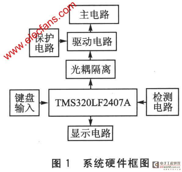
Figure 1 is a block diagram of the system hardware. In this system, TMS320LF2407A is used as the main control chip, and the inverter uses SPWM modulation control to implement the variable frequency control algorithm. The system hardware consists of the main circuit, display circuit, keyboard input circuit, and detection and protection circuit. The DSP first collects the required frequency signal from the keyboard, then generates the corresponding SPWM signal through calculation, transmits it to the drive circuit through the optical coupler, and then controls the power tube in the inverter bridge to turn on and off. At the same time, it collects relevant signals in the main circuit and determines whether there is a fault output. If there is a fault, the SPWM output of the DSP is turned off, thereby turning off the main circuit.
2.1 Main circuit composition
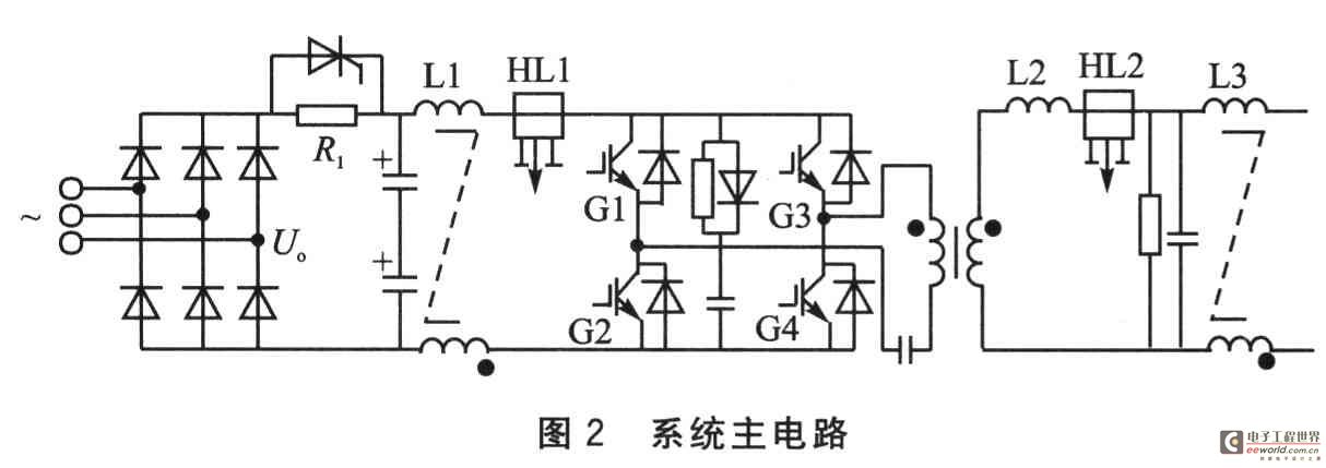
Figure 2 shows the main circuit of the system, which consists of three parts: rectifier circuit, filter circuit and inverter circuit. The rectifier circuit is a three-phase uncontrolled rectifier bridge, which rectifies 380 V, 50 Hz AC into pulsating DC. The circuit uses filter capacitors for filtering to remove voltage ripples. At the same time, the filter capacitor also plays a decoupling role between the rectifier circuit and the inverter to eliminate mutual interference. The average value of the rectified DC voltage is UO=1.35U2≈1.4U2=540 V. U2 is the effective value of the AC side voltage. Considering that the input three-phase power has a 10% fluctuation, UO=500~560 V. The power devices G1, G2, G3, and G4 in the main circuit diagram represent IGBT devices, whose model is MG50Q2YS40, with a withstand voltage of 1,200 V, a control voltage of 20 V, and a current of 50 A. R1 is a current limiting resistor to prevent the impact current from damaging the IGBT. L1 and L3 are common mode filters, HL1 and HL2 are current Hall elements, which are used to detect the current value of the main circuit as the input signal of the protection circuit; in addition, voltage Hall elements are used to detect the voltage value as the input signal of the protection circuit and the voltage feedback signal, forming voltage negative feedback. The four IGBTs controlled by SPWM technology are used for inversion. The output AC power is transformed by the transformer and then filtered by the LC filter to output 220 V variable frequency AC power.
2.2 Driving and protection circuit
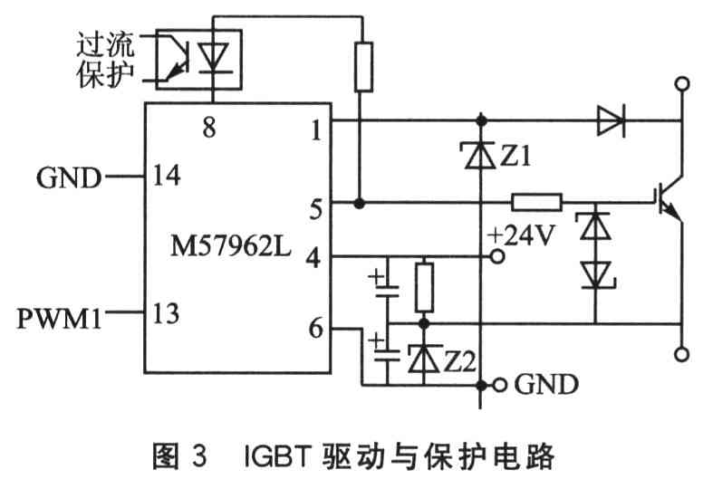
Figure 3 shows the principle of the drive circuit. The inverter circuit power device of this system uses IGBT chips, so the drive circuit uses 4 M57962L drive modules produced by Mitsubishi. The drive module is a hybrid integrated circuit that integrates the drive and overcurrent protection of the IGBT. In Figure 3, the 13th pin of the M57962L is connected to the PWM1 of the DSP (the other 3 M57962Ls are connected to PWM2, PWM3, and PWM4 respectively), the 14th pin is grounded, and the 1st and 6th pins are connected to the power supply respectively. In addition, the M57962L uses a low voltage drive, that is, the M57962L can only be driven when the 13th pin inputs a negative potential. The advantage of this is that it prevents interference. When an interference waveform appears, the M57962L driven by a low level cannot be driven. In addition, during the shutdown process, if the voltage changes too much, a holding phenomenon will occur, causing the IGBT to lose control and causing the upper and lower bridge arms to pass directly. Therefore, an RC buffer circuit is used to suppress overvoltage and voltage change rate du/dt.
3 Digital Implementation of the System
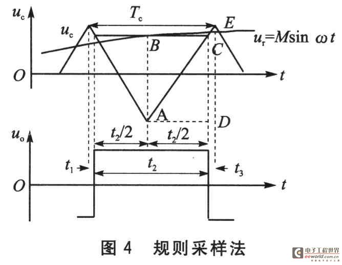
The inverter part of the system adopts the SPWM regular sampling algorithm, and its basic idea is to make the output pulse change according to the sinusoidal law, so as to reduce the harmonic components in the output voltage and make the output voltage closer to a sine wave. In order to facilitate digital implementation, the SPWM pulse sequence is generated by the regular sampling method, and its principle is shown in Figure 4. Because the triangular carrier frequency is much higher than the sine wave frequency, the sinusoidal modulation wave ut within one cycle of the triangular carrier uc is regarded as unchanged. In this way, in one triangular wave cycle, only one sampling at point B is required to make the midpoint of the generated SPWM pulse coincide with the midpoint of the corresponding triangular wave (point A), thereby greatly simplifying the calculation of the SPWM pulse. Assume that the amplitude of uc is 1, and the sinusoidal modulation signal ut=Msinωtt, where O≤M<1 (M is the modulation index). Since △ABC~△EDA, we have:
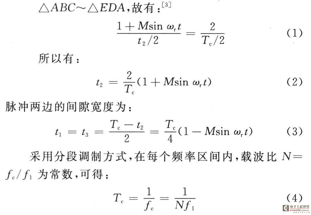
The sine function value is obtained by table lookup. In addition, N is taken as a multiple of 3 in each segment of synchronous modulation.
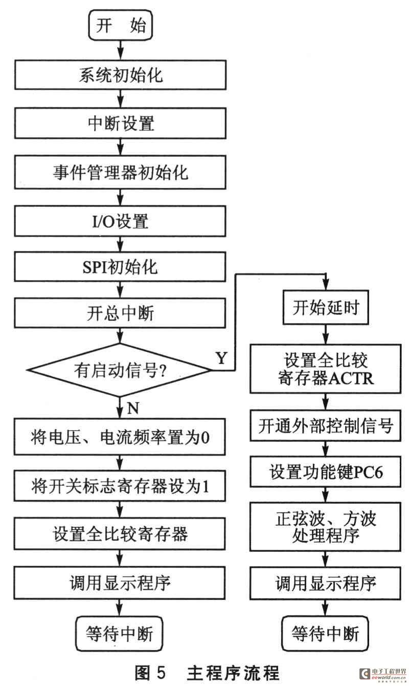
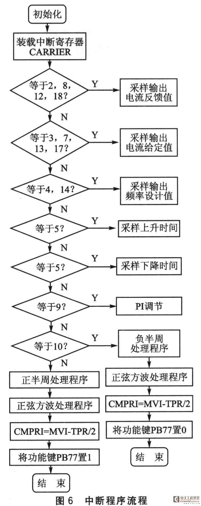
Software programming is the core of inverter control circuit design. The system software mainly includes: main program, interrupt service program, PI adjustment program, display program, etc. Figure 5 is the main program flow, and Figure 6 is the interrupt program flow. In the main program, the DSP system and external device initialization, I/O control signal management, and sine wave signal generation and processing are completed. In the interrupt program, current and voltage detection, PI adjustment calculation, calculation of modulation degree M and frequency value under constant voltage-frequency ratio, sine wave processing and assignment of comparator CMPRl are completed.
4 Experimental Results
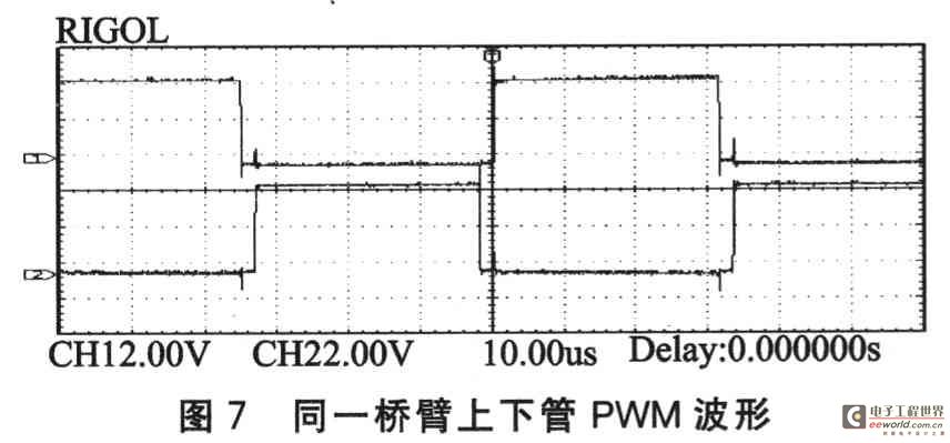
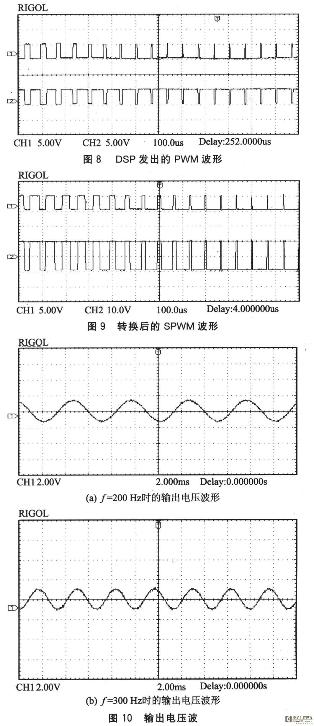
Figure 7 shows the waveforms of PWM1 and PWM2 of the upper and lower tubes of the same bridge arm. As can be seen from the figure, a dead time of 2μs is set for the upper and lower bridge arms to ensure the safe operation of the inverter circuit. Figure 8 shows the PWM waveform issued by the DSP, (1) and (2) are two complementary pulse signals of equal amplitude and unequal width. The high level is +5 V, the low level is 0V, and the pulse width changes according to the sine law. Since the M57962L chip uses a negative potential drive, a level conversion circuit is required. Figure 9 shows the SPWM waveform of the final drive IGBT (the converted SPWM waveform). It can be seen from the figure that the width of the waveform changes according to the sine law. Figure 10 (a) and (b) are the output voltage waveforms at f=200 Hz and f=300 Hz respectively. The experimental results show that the output voltage waveform has good quality and low total harmonic distortion.
5 Conclusion
Digital control technology based on DSP can greatly improve the consistency of products, overcome the dispersion of product performance caused by analog control, and enhance the flexibility of control, simplify the system structure, improve the stability and reliability of the entire system, and have good application prospects. This design uses the TMS320LF2407A chip and SPWM control technology to transform the 380 V, 50 Hz AC power supply into an output 220 V, 100-400 Hz adjustable AC power supply. The actual measurement of the prototype shows that the output waveform quality is good, overcoming the shortcomings of large noise, slow response, and severe waveform distortion that occurred when this type of power supply used a large medium-frequency transformer in the past. It is a product with good application prospects.
Previous article:Design of Satellite Remote Sensing Image Compression System Based on Multi-DSP+FPGA
Next article:DSP Parallel Boot Loading Method Based on Flash Memory
Recommended ReadingLatest update time:2024-11-16 21:22


- Popular Resources
- Popular amplifiers
- Huawei's Strategic Department Director Gai Gang: The cumulative installed base of open source Euler operating system exceeds 10 million sets
- Analysis of the application of several common contact parts in high-voltage connectors of new energy vehicles
- Wiring harness durability test and contact voltage drop test method
- Sn-doped CuO nanostructure-based ethanol gas sensor for real-time drunk driving detection in vehicles
- Design considerations for automotive battery wiring harness
- Do you know all the various motors commonly used in automotive electronics?
- What are the functions of the Internet of Vehicles? What are the uses and benefits of the Internet of Vehicles?
- Power Inverter - A critical safety system for electric vehicles
- Analysis of the information security mechanism of AUTOSAR, the automotive embedded software framework
 Professor at Beihang University, dedicated to promoting microcontrollers and embedded systems for over 20 years.
- Innolux's intelligent steer-by-wire solution makes cars smarter and safer
- 8051 MCU - Parity Check
- How to efficiently balance the sensitivity of tactile sensing interfaces
- What should I do if the servo motor shakes? What causes the servo motor to shake quickly?
- 【Brushless Motor】Analysis of three-phase BLDC motor and sharing of two popular development boards
- Midea Industrial Technology's subsidiaries Clou Electronics and Hekang New Energy jointly appeared at the Munich Battery Energy Storage Exhibition and Solar Energy Exhibition
- Guoxin Sichen | Application of ferroelectric memory PB85RS2MC in power battery management, with a capacity of 2M
- Analysis of common faults of frequency converter
- In a head-on competition with Qualcomm, what kind of cockpit products has Intel come up with?
- Dalian Rongke's all-vanadium liquid flow battery energy storage equipment industrialization project has entered the sprint stage before production
- Allegro MicroSystems Introduces Advanced Magnetic and Inductive Position Sensing Solutions at Electronica 2024
- Car key in the left hand, liveness detection radar in the right hand, UWB is imperative for cars!
- After a decade of rapid development, domestic CIS has entered the market
- Aegis Dagger Battery + Thor EM-i Super Hybrid, Geely New Energy has thrown out two "king bombs"
- A brief discussion on functional safety - fault, error, and failure
- In the smart car 2.0 cycle, these core industry chains are facing major opportunities!
- The United States and Japan are developing new batteries. CATL faces challenges? How should China's new energy battery industry respond?
- Murata launches high-precision 6-axis inertial sensor for automobiles
- Ford patents pre-charge alarm to help save costs and respond to emergencies
- New real-time microcontroller system from Texas Instruments enables smarter processing in automotive and industrial applications
- Global reset (GSR) in FPGA development
- [Gizwits Gokit3 Review] Device access-Step 3: Download the program firmware
- When a PCB designer encounters love, guess how much the impedance of his board changes
- Iwatch Apple Watch Wireless Charging
- Practical sharing: A collection of 5G manuscripts by frontline engineers
- New Forum Homepage User Guide
- Please help me with some questions about using AD for beginners
- Ultimate Electronics
- EEWORLD University ----TI Automotive Instrument Solutions
- CC2541 Bluetooth Watchdog Mode

 Power Electronics Technology (Editor-in-Chief: Wang Luyang; Deputy Editor-in-Chief: Wang Hexing)


 京公网安备 11010802033920号