1. Introduction to I2S
I2S stands for Inter-IC Sound, Integrated Interchip Sound, or IIS for short. It is a digital audio transmission standard defined by Philips in 1986 (revised in 1996) for transmitting digital audio data between internal components of a system, such as CODEC, DSP, digital input/output interface, ADC, DAC, and digital filter. I2S has nothing to do with I2C except that both were defined by Philips.
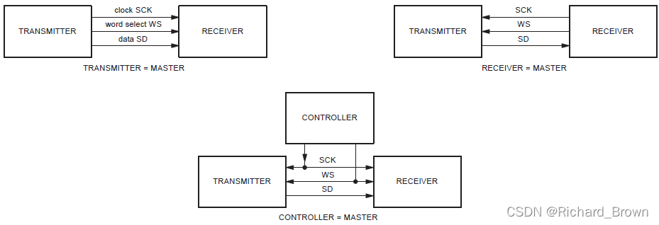
I2S is a relatively simple digital interface protocol without address or device selection mechanism. On the I2S bus, there can only be one master device and one sending device at the same time. The master device can be a sending device, a receiving device, or other control device that coordinates the sending device and the receiving device. In the I2S system, the device that provides the clock (SCK and WS) is the master device. Figure 3 is a common I2S system block diagram. In high-end applications, CODEC is often used as the master device of I2S to accurately control the data flow of I2S.

I2S includes two channels (Left/Right) of data, and the left and right channels are switched under the control of channel selection/word selection (WS) issued by the master device. Multi-channel applications can be realized by increasing the number of I2S interfaces or other I2S devices.
2. Signal Definition
In the I2S transmission protocol, data signals, clock signals, and control signals are transmitted separately. The I2S protocol only defines three signal lines: clock signal SCK, data signal SD, and left and right channel selection signal WS.
Serial Clock
SCK is the synchronization signal within the module. It is provided by the outside in slave mode and generated by the module itself in master mode. The clock signal may be called differently for different chip models from different manufacturers. It may also be called BCLK/Bit Clock or SCL/Serial Clock.
Serial Data
SD is serial data, which is transmitted on the data line in the form of binary complement in I2S. In the first SCK pulse after WS changes, the most significant bit (MSB) is transmitted first. The MSB is transmitted first because the word length of the sending device and the receiving device may be different. When the system word length is longer than the word length of the data sending end, the data transmission will be truncated/Truncated, that is, if the data bit received by the data receiving end is longer than the specified word length, then all bits after the specified word length least significant bit (LSB: Least Significant Bit) will be ignored. If the received word length is shorter than the specified word length, the remaining bits will be filled with 0. In this way, the most significant bit of the audio signal can be transmitted, thereby ensuring the best auditory effect.
Depending on the input or output characteristics, SD on different chips may also be called SDATA, SDIN, SDOUT, DACDAT, ADCDAT, etc.;
Data transmission can be synchronized with the rising edge or falling edge of SCK, but the receiving device samples on the rising edge of SCK, and the timing of sending data needs to be considered.
Left and right channel selection signal Word Select
WS is the channel selection signal, indicating the channel selected by the data transmitter.
WS=0, indicating the left channel is selected
WS=1, indicating the right channel is selected
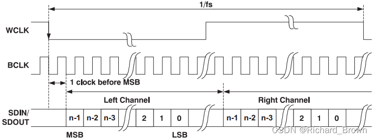
WS is also called frame clock, i.e. LRCLK/Left Right Clock. The WS frequency is equal to the sampling rate of the sound. WS can change on the rising edge of SCK or on the falling edge of SCK. The slave device samples the WS signal on the rising edge of SCK. The data signal MSB is valid on the rising edge of the second clock (SCK) after WS changes (i.e. delayed by one SCK), which allows the slave device enough time to store the currently received data and prepare to receive the next set of data.
3. I2S Operation Mode
Depending on the position of SD relative to SCK and WS, I2S is divided into three different operating modes: standard I2S mode, left-aligned mode, and right-aligned mode:
I2S Phillips Standard I2S format
Left JusTIfied Standard Left justified format
Right JusTIfied Standard Right justified format
I2S mode is a special case of left alignment, also called PHILIPS mode, which is a change from the standard left alignment format with one clock bit delayed. The timing is shown in the figure below. The MSB of the left channel data is valid on the second SCK/BCLK rising edge after the WS falling edge, and the MSB of the right channel data is valid on the second SCK/BCLK rising edge after the WS rising edge.

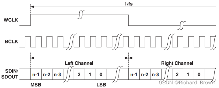
Standard left alignment is rarely used. The following figure is a left alignment timing diagram. Compared with the PHILIPS format, it can be seen that the MSB of the data in the standard left alignment format is not delayed by one clock relative to BCLK. The MSB of the left channel data in the left alignment format is valid at the first rising edge of SCK/BCLK after the rising edge of WS; the MSB of the right channel data is valid at the first rising edge of SCK/BCLK after the falling edge of WS. The advantage of the standard left alignment format is that since sampling starts at the first SCK rising edge after the WS changes, it does not need to care about the word length of the left and right channel data. As long as the clock cycle of WS is long enough, the left alignment method supports 16-32bit word length format.

Standard right alignment is also called Japanese format, EIAJ (Electronic Industries Association of Japan) or SONY format. The following figure is a right alignment timing diagram. In the right alignment format, the data LSB of the left channel is valid on the SCK/BCLK rising edge before the WS falling edge, and the data LSB of the right channel is valid on the SCK/BCLK rising edge before the WS rising edge. Compared with the standard left alignment format, the disadvantage of the standard right alignment is that the receiving device must know the word length of the data to be transmitted in advance. This also explains why many CODECs provide multiple right alignment format selection functions.
Note:
The left and right channels corresponding to the LRCK/WS high and low levels in the standard left-aligned and standard right-aligned modes are exactly opposite to those in the standard I2S mode! The standard left-right aligned LRCK/WS high level corresponds to the left channel, and the LRCK/WS low level corresponds to the right channel; while the I2S low level corresponds to the left channel, and the LRCK/WS high level corresponds to the right channel!
4. I2S data clock (SCK) frequency calculation
For example, if the sampling frequency of the sound is 44.1 kHz, the frequency of the channel selection signal (frame clock) WS must also be 44.1 kHz; the quantization depth of the left/right channels is 16 bits, then the frequency of I2S SCK is: 44.1 kHz×16×2=1.4112 MHz
SCK = sampling rate * bit width * number of channels
WS = Sampling rate
If you need to transmit 20-bit, 24-bit or 32-bit left and right channel data, you can increase the SCK frequency. The required SCK frequency can be calculated from the above formula.
PCM Interface
1. Introduction to PCM
PCM (Pulse Code Modulation) is a method of digitizing analog signals by sampling at equal time intervals (i.e., sampling rate clock cycles). The following figure is a schematic diagram of PCM data quantization with a sampling depth of 4 bits.

PCM digital audio interface means that the audio data transmitted on the interface is sampled by PCM method, which is different from PDM method. In the audio field, PCM interface is often used for the transmission of board-level audio digital signals, similar to I2S. The difference between PCM and I2S lies in the position of data relative to the frame clock (FSYNC/WS), the polarity of the clock and the length of the frame. In fact, the data transmitted on I2S is also PCM type data, so it can be said that I2S is just a special case of PCM interface.
Compared with the I2S interface, the PCM interface is more flexible to use. Through time division multiplexing (TDM), the PCM interface supports the simultaneous transmission of up to N (N>8) channels of data, reducing the number of pins (actually reducing the number of "groups" of I2S, because each group of I2S can only transmit two channels of data). TDM does not have a unified standard like I2S. Different IC manufacturers may have slight differences in the application of TDM. These differences are reflected in the polarity of the clock, the trigger conditions of the channel configuration, and the processing of idle channels.
The hardware topology of the TDM/PCM digital audio interface is also similar to that of I2S.
After reviewing the data sheets of many manufacturers, I found that when a PCM audio interface is used to transmit mono data (such as a microphone), the interface name is PCM; I2S is often used for dual channels; and TDM indicates the transmission of data for two or more channels, which is different from the specific format of I2S.
2. Signal Definition
The PCM interface is similar to I2S, and the circuit signals include:
PCM_CLK Data clock signal
PCM_SYNC frame synchronization clock signal
PCM_IN receives data signal
PCM_OUT sends data signal
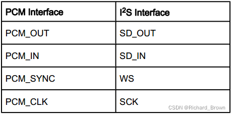
The corresponding relationship between TDM/PCM and I2S interface is shown in the following table:

3. Operation Mode
According to the position of SD relative to the frame synchronization clock FSYNC, TDM is divided into two basic modes:
Mode A: Data is valid on the second rising edge of BCLK after FSYNC is valid
Mode B: Data is valid on the first rising edge of BCLK after FSYNC is valid


Note: Due to the lack of a unified standard, different manufacturers may have different definitions of Mode A and Mode B.
In practical applications, the rising edge of the frame synchronization clock FSYNC always indicates the start of a transmission. The frequency of the frame synchronization clock is always equal to the audio sampling rate, such as 44.1 kHz, 48 kHz, etc. Most applications only use the rising edge of FSYNC and ignore its falling edge. According to the difference in FSYNC pulse width in different applications, PCM frame synchronization clock modes are roughly divided into two types:
Previous article:What circuit is used to realize the button function of the TV?
Next article:Why does the home air conditioner encounter the E1 fault code?
Recommended ReadingLatest update time:2024-11-16 14:50
- Huawei's Strategic Department Director Gai Gang: The cumulative installed base of open source Euler operating system exceeds 10 million sets
- Analysis of the application of several common contact parts in high-voltage connectors of new energy vehicles
- Wiring harness durability test and contact voltage drop test method
- Sn-doped CuO nanostructure-based ethanol gas sensor for real-time drunk driving detection in vehicles
- Design considerations for automotive battery wiring harness
- Do you know all the various motors commonly used in automotive electronics?
- What are the functions of the Internet of Vehicles? What are the uses and benefits of the Internet of Vehicles?
- Power Inverter - A critical safety system for electric vehicles
- Analysis of the information security mechanism of AUTOSAR, the automotive embedded software framework
 Professor at Beihang University, dedicated to promoting microcontrollers and embedded systems for over 20 years.
- Innolux's intelligent steer-by-wire solution makes cars smarter and safer
- 8051 MCU - Parity Check
- How to efficiently balance the sensitivity of tactile sensing interfaces
- What should I do if the servo motor shakes? What causes the servo motor to shake quickly?
- 【Brushless Motor】Analysis of three-phase BLDC motor and sharing of two popular development boards
- Midea Industrial Technology's subsidiaries Clou Electronics and Hekang New Energy jointly appeared at the Munich Battery Energy Storage Exhibition and Solar Energy Exhibition
- Guoxin Sichen | Application of ferroelectric memory PB85RS2MC in power battery management, with a capacity of 2M
- Analysis of common faults of frequency converter
- In a head-on competition with Qualcomm, what kind of cockpit products has Intel come up with?
- Dalian Rongke's all-vanadium liquid flow battery energy storage equipment industrialization project has entered the sprint stage before production
- Allegro MicroSystems Introduces Advanced Magnetic and Inductive Position Sensing Solutions at Electronica 2024
- Car key in the left hand, liveness detection radar in the right hand, UWB is imperative for cars!
- After a decade of rapid development, domestic CIS has entered the market
- Aegis Dagger Battery + Thor EM-i Super Hybrid, Geely New Energy has thrown out two "king bombs"
- A brief discussion on functional safety - fault, error, and failure
- In the smart car 2.0 cycle, these core industry chains are facing major opportunities!
- The United States and Japan are developing new batteries. CATL faces challenges? How should China's new energy battery industry respond?
- Murata launches high-precision 6-axis inertial sensor for automobiles
- Ford patents pre-charge alarm to help save costs and respond to emergencies
- New real-time microcontroller system from Texas Instruments enables smarter processing in automotive and industrial applications
- Triangle wave generating circuit
- [RT-Thread Reading Notes] Part 2 (1) Porting, Running and Thread Management
- Are you confused about gate driver selection? Download the latest selection guide
- Wish you all a happy Dragon Boat Festival
- Using MCU to implement speech recognition? MSP432 can do it!
- Lead Angle/Conduction Angle of Brushless DC Motor
- FIR filter design based on FPGA (source code download attached)
- The timing relationship between voltage and current lead and lag
- LSM6DSO MicroPython driver porting
- Keil C51 MCU Programming Software and Instructions Learning Tutorial (Full Version)


 Siemens PLC from Beginner to Mastery with Color Illustrations (Yang Rui)
 Siemens S7-1200-PLC Programming and Application Tutorial (3rd Edition) (Edited by Shi Shouyong)
 ESP32-S3 source code


 京公网安备 11010802033920号