Gigabit network interface has the advantages of fast data transmission rate, convenient connection and plug-and-play, which makes it widely used. With the development of electronic technology and processors, the data communication rate of many applications exceeds the actual transmission rate of Gigabit network port. For example, in A/D sampling, it is necessary to directly store the sampled data of A/D conversion. If the A/D conversion bit number is 16 bits and it works at 100MHz, the actual data volume is 1.6Gbps. In order to achieve high-speed transmission, an interface with a higher transmission rate must be used, such as PCIe or RapidIO interface. However, these interfaces do not have plug-and-play functions and cannot be directly connected to many existing industrial equipment, which limits their application scenarios.
DSP (digital signal processor) has a high operating frequency, and its internal hardware network MAC interface is integrated. It can easily realize Gigabit network communication by connecting an external physical layer chip. Multi-core DSP chips can connect multiple Gigabit network ports, making them applicable to high-speed data transmission occasions. This article introduces an embedded dual Gigabit network interface based on the multi-core digital signal processor TMS320C6678, which realizes the connection of two Gigabit network ports with a single chip. These two network ports can transmit data independently or jointly, which improves the actual data transmission rate.
1. C6678 and its structure
TMS320C6678 is an 8-core floating-point DSP in TI's multi-core processors. Each core has a maximum operating frequency of 1.25GHz. Each core can provide 40GMAC fixed-point computing or 20GFLOP floating-point computing capabilities. A single chip can provide 320GMAC or 160GFLOP computing capabilities. The on-chip structure of TMS320C6678 is shown in Figure 1.
Each core of TMS320C6678 has 32KB of program, 32KB of data and 512KB of 2nd level cache storage space, and a 4MB shared SRAM inside the chip. TMS320C6678 has a DDR3 controller interface, which can be connected to DDR3 externally, and the direct addressing range reaches 8GB. TMS320C6678 has RapidIO, PCIe, EMIF, SPI, I2 C bus and other interfaces inside and outside the chip. These interfaces exchange data with each processor through the high-speed interconnect bus inside the chip.
The network-related on-chip devices are shown in the gray module in the lower right corner of Figure 1. They mainly include two external SGMII interfaces, Ethernet switching and network switching modules, as well as security accelerators and packet accelerators for data management. They can quickly detect data verification and whether the protocol complies with network standards, and directly discard erroneous data to reduce the burden on the CPU. In order to speed up the data exchange between the network and the CPU, the on-chip queue manager is used to manage the cache and distribution of network packets or network frames. These data are read and written using data packet DMA, and do not require CPU participation.
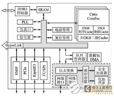
Figure 1 TMS320C6678 internal structure
Other on-chip devices of TMS320C6678 include PLL, emulation port, semaphore, power management and reset management modules. PLL configures the working clock of CPU and peripherals; emulation port is used to connect emulator to monitor software operation; semaphore controls the semaphore in DSP/BIOS operating system; power management controls the current and voltage of the whole chip; reset management configures the startup mode, hard reset for full startup and soft reset for partial startup.
2. 88E1111 and its structure
There are many network physical layer chips, which are generally compatible with one or more interface standards such as MII, RMII and SGMII. However, TMS320C6678 only provides SGMII interface, so the physical layer chip connected to TMS320C6678 must have SGMII interface. This article uses two Marvell 88E1111 physical layer chips to connect dual Gigabit networks. The internal structure of 88E1111 is shown in Figure 2.

Figure 2 88E1111 internal structure
The analog signal with modulated data sent from the network RJ45 interface is converted into a digital signal through A/D conversion, and then transmitted to the MAC chip by the receiving unit after being equalized, shaped and filtered, and decoded in sequence to realize data reception. The data sent by the MAC is converted into an analog signal by D/A after being shaped and filtered and sent to the RJ45 interface. In order to reduce the bit error rate, the 88E1111 has modules such as phase-locked loop (PLL), automatic gain control (AGC), timing/phase control, and echo cancellation. These modules are all designed to improve the reliability of data transmission, and can communicate reliably and at high speed in different environments or with different external devices. The LED control module in Figure 2 realizes the light display during data transmission, the MDIO module realizes link establishment and status monitoring, and the clock module provides the working clock.
3. Hardware Design
The hardware design mainly includes the interface between TMS320C6678 and two 88E1111s, the interface between 88E1111 and RJ45, and the hardware configuration design of 88E1111.
The network module structure of TMS320C6678 is shown in Figure 3. A 3-port Ethernet switch is integrated in the chip, which is responsible for exchanging data from two Gigabit Ethernet ports to the host and providing exchange interrupts to the host. The host can receive and send data in real time through interrupts. The host configures or monitors the external physical layer chip through the bus, and the configuration and monitoring data are connected to the physical layer chip through the MDIO interface.
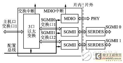
Figure 3 TMS320C6678 network module structure
Figure 4 Interface between TMS320C6678 and 88E1111 The interface circuit between TMS320C6678 and two 88E1111s is shown in Figure 4. TMS320C6678 uses SGMII (Serial Gigabit Media Independent Interface) interface, which is compatible with 10/100/1000M working mode. SGMII is a serial data transceiver mode with fewer pin connections. As can be seen from Figure 4, there are actually only two pairs of differential lines for transceiver, which are connected to the corresponding 88E1111 pins respectively. The read and write clocks are implicitly transmitted in the data and are automatically recognized by the hardware without the need for software participation.
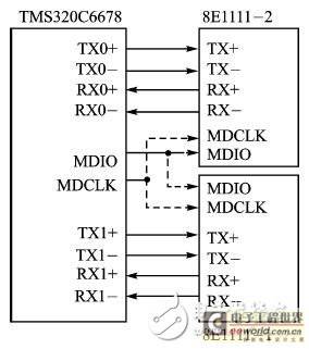
Figure 4 Interface between TMS320C6678 and 88E1111
MDIO and MDCLK are the data and clock of the MDIO module inside TMS320C6678, which are used to establish a connection between TMS320C6678 and 88E1111. TMS320C6678 can configure 88E1111 through this interface, or read the information of 88E1111. Since the MDIO module interface level of 88E1111 is 2.5V, and the MDIO module interface level of TMS320C6678 uses 1.8V voltage, a voltage conversion chip needs to be added between the two. This design uses PCA9306 to achieve voltage conversion. The interface circuit is shown in Figure 5.
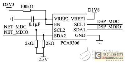
Figure 5 MDIO interface voltage conversion circuit
It should be noted that since there are two 88E111 chips, the MDIO and MDCLK pins are directly connected to the two chips. MDIO can control up to 32 physical layer chips, and the physical layer chip addresses are 1 to 32. The address configuration of 88E1111 is shown in Figure 6.
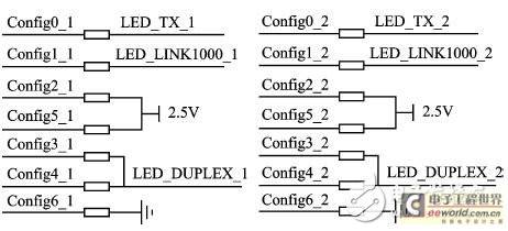
Figure 6 88E1111 hardware configuration
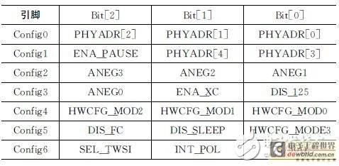
Table 1 is the corresponding configuration information. According to FIG. 6 and Table 1, it can be seen that the addresses of 88E111 are 4 and 8 respectively.
Table 1 Configuration pin settings
4. Software Design
The system software design includes hardware initialization, network configuration, and data communication process. The workflow of TMS320C6678 after reset is shown in Figure 7. First, configure the first network port, record its status, and then configure the second network port. As long as one of the two network ports is successfully configured, the EMAC module of TMS320C6678 will be configured to set the transceiver buffer and transceiver tasks for the successfully configured network port. After these configurations are completed, network data transmission and reception can be realized. It should be noted that in the user application, the failure of network port configuration needs to be considered. For example, the user application transmits 1.2Gbps data in real time through dual network ports. If one network port configuration fails, the application should have a corresponding mechanism to reduce the real-time transmission rate to less than 0.8Gbps (the actual transmission rate of a single network port may be lower than 0.8Gbps). In the absence of other task overhead, the hardware system in this article can transmit 1.5Gbps of data (errors are not considered during transmission and retransmission is not performed).
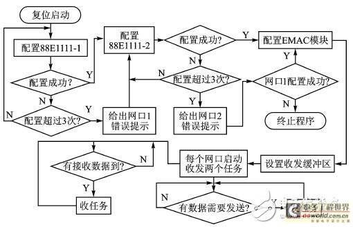
Figure 7 Data communication process
Conclusion
Communication interfaces with a transmission rate exceeding 1Gbps generally use optical fiber, PCE, PCIe and other interface methods. This article uses a dual network port method to reduce equipment requirements and facilitate connection with existing equipment. The use of multi-core DSP improves the processor's working ability. While ensuring the large-capacity data transmission process, the processor still has the ability to calculate data. The dual network port design can make up for the insufficient transmission rate of a single network port and reduce the hardware complexity of other interfaces. It is a beneficial supplement between the two. It has certain application value in embedded devices.
Previous article:In-depth analysis of DSP electromagnetic compatibility issues
Next article:The core DSP device of embedded system technology
Recommended ReadingLatest update time:2024-11-16 22:27


- Popular Resources
- Popular amplifiers
- Huawei's Strategic Department Director Gai Gang: The cumulative installed base of open source Euler operating system exceeds 10 million sets
- Analysis of the application of several common contact parts in high-voltage connectors of new energy vehicles
- Wiring harness durability test and contact voltage drop test method
- Sn-doped CuO nanostructure-based ethanol gas sensor for real-time drunk driving detection in vehicles
- Design considerations for automotive battery wiring harness
- Do you know all the various motors commonly used in automotive electronics?
- What are the functions of the Internet of Vehicles? What are the uses and benefits of the Internet of Vehicles?
- Power Inverter - A critical safety system for electric vehicles
- Analysis of the information security mechanism of AUTOSAR, the automotive embedded software framework
 Professor at Beihang University, dedicated to promoting microcontrollers and embedded systems for over 20 years.
- Innolux's intelligent steer-by-wire solution makes cars smarter and safer
- 8051 MCU - Parity Check
- How to efficiently balance the sensitivity of tactile sensing interfaces
- What should I do if the servo motor shakes? What causes the servo motor to shake quickly?
- 【Brushless Motor】Analysis of three-phase BLDC motor and sharing of two popular development boards
- Midea Industrial Technology's subsidiaries Clou Electronics and Hekang New Energy jointly appeared at the Munich Battery Energy Storage Exhibition and Solar Energy Exhibition
- Guoxin Sichen | Application of ferroelectric memory PB85RS2MC in power battery management, with a capacity of 2M
- Analysis of common faults of frequency converter
- In a head-on competition with Qualcomm, what kind of cockpit products has Intel come up with?
- Dalian Rongke's all-vanadium liquid flow battery energy storage equipment industrialization project has entered the sprint stage before production
- Allegro MicroSystems Introduces Advanced Magnetic and Inductive Position Sensing Solutions at Electronica 2024
- Car key in the left hand, liveness detection radar in the right hand, UWB is imperative for cars!
- After a decade of rapid development, domestic CIS has entered the market
- Aegis Dagger Battery + Thor EM-i Super Hybrid, Geely New Energy has thrown out two "king bombs"
- A brief discussion on functional safety - fault, error, and failure
- In the smart car 2.0 cycle, these core industry chains are facing major opportunities!
- The United States and Japan are developing new batteries. CATL faces challenges? How should China's new energy battery industry respond?
- Murata launches high-precision 6-axis inertial sensor for automobiles
- Ford patents pre-charge alarm to help save costs and respond to emergencies
- New real-time microcontroller system from Texas Instruments enables smarter processing in automotive and industrial applications
- COVID-19 and other challenges to LED design and coping strategies
- purchase
- Shocked! One person made a company popular
- [Liquid Level Sensor Evaluation] A/D Data Acquisition and Numerical Display
- [Evaluation of EC-01F-Kit, the NB-IoT development board of Anxinke] + Try to connect the serial port assistant to Alibaba Cloud
- [Jihai APM32E103VET6S MINI Development Board Review] Part 4: Key Interrupt
- Technology Popularization: Do you know why base stations are painted in colors?
- Usage of ^ in Verilog
- A brief list of long and short distance wireless communication technologies
- A classic foreign book about semaphores

 MATLAB and FPGA implementation of wireless communication


 京公网安备 11010802033920号