Data acquisition occupies an irreplaceable position in the information processing system. It is formed based on technologies such as sensors, signal measurement and processing, and microcomputers. It mainly studies the acquisition, storage, processing, and control of information data, and has strong practicality. Data acquisition technology has been widely used in many fields such as radar, communication, underwater acoustics, remote sensing, speech processing, intelligent instruments, industrial automation, and biomedical engineering. Data collectors generally include data acquisition parts and data processing and transmission parts. The former includes signal filtering, amplification, sampling, holding, conversion, storage, etc., and the latter includes data reading, transmission, and microcomputer interface parts.
1 System structure and hardware circuit design
1.1 System structure diagram and working principle
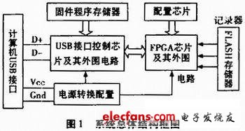
This system is mainly composed of four modules: FLASH memory module, FPGA control module, USB interface control module and power module, as shown in Figure 1.

Its working principle is: the FLASH module stores data as the data source of the recorder; the FPGA module acts as the controller of the reading device, reads the FLASH data and transmits it to the USB control interface module; the USB control chip receives commands from the host computer and communicates with the FPGA to perform the operations required by the user; the power module provides stable power for each module.
1.2 Power Management Module
The operating voltages of the chips in this system are 5 V, 3.3 V, and 2.5 V. Since the USB interface of the computer can provide a 5 V power supply with a maximum current of 500 mA, which is sufficient for this system, the 5 V power supply of this system is directly powered by the USB, and the 5 V power supply is adjusted to 3.3 V and 2.5 V power supplies through the voltage regulator AMS1117.
1.3 FPGA module
The FPGA of this design adopts XC2S50 of Spartan-2 series of XILINX company, including FPCA configuration circuit and FPGA clock circuit and interface configuration.
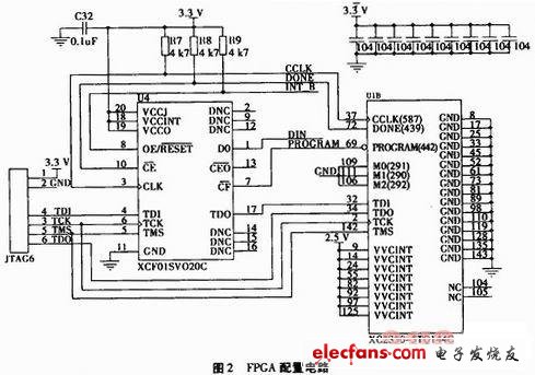
FPGA has flexible and diverse configuration methods. This design uses the master string mode to configure FPCA based on whether the chip can actively load configuration data and the bit width of the bit stream, as shown in Figure 2. A resistor is connected to each port on the output port of the FPGA to play the role of coupling current limiting, so that the external interface matches the FPGA to prevent the chip from burning out due to adverse effects such as excessive current.

1.4 USB interface module
Generally speaking, the types of USB interface chips can be roughly divided into: host controller, root hub, interface chip and microcontroller with USB interface. This design uses the CY7C68013A-128PIN chip of the EZ-USB FX2LP series.
This design uses the EEPROM boot mode of 0XC0. That is, write 0XC0 to the first byte in the EEPROM, and write VID, PID, DID and configuration bytes to the EEPROM. After the chip is powered on, these data are copied to the on-chip memory and sent to the host, which selects the appropriate firmware program based on the ID data and downloads it to the USB chip. This design uses the serial EEPROM chip AT24C64 with an I2C bus interface. AT24C64 has a capacity of 8192 x 8 bits and can be repeatedly erased 1 million times.
1.5 FLASH memory module
The FLASH memory stores the data of the recorder. The purpose of this design is to read the data from the FLASH and transfer it to the computer for storage. This design uses the K9F5608UOD NAND FLASH memory of SAMSUNG. Its features are as follows: the storage cell array is (32M+1024k)bit×8bit; a total of 64k blocks, each block contains 32 pages, and each page is 512+16 bytes; programming in pages (200μs typical programming time), erasing in blocks (2ms typical erasing time); command, address, and data multiplexing ports; providing hardware data protection function.

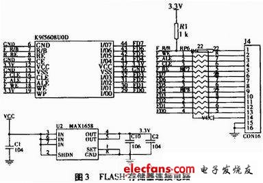
The hardware connection circuit of this design is shown in Figure 3. The MAX1658 provides power for the K9F5608UOD, and the resistor plays a coupling and current limiting role.
2 Software Programming
2.1 FPGA module programming
The FPGA program of this design adopts ISE software of Xilinx Company. It provides users with a complete solution from design input to synthesis, routing, simulation and download, and can be easily interfaced with other EDA tools.
In this design, the schematic input uses the third-party software ECS, HDL synthesis uses XST, the test bench input is the graphical HDL Bencher, and the simulation uses Modelsim SE. The brief process is as follows:
Create an engineering project; synthesize; simulate; define input and output pin constraints; layout and routing; download configuration.
In the FLASH module programming, the FLASH control module performs various operations on the FLASH memory K9F5608UOD. The K9F5608UOD chip provides 8 commands, namely 8 operations: ① read 1 operation; ② read 2 operation; ③ read ID operation; ④ reset operation; ⑤ page programming operation; ⑥ copy readback operation; ⑦ block erase operation; ⑧ read status operation.
2.2 CY7C68013 firmware development
The hardware functions of USB functional devices are mainly realized by the microprocessor on the hardware, so it is necessary to write firmware programs for USB devices. In the development of USB firmware programs in this design, Keil μVision3, a 51 series compatible microcontroller software development system launched by Keil Software, is used.

Figure 4 shows the firmware program flow chart of 68013A. The following describes how to program. This design uses the Dscr.a51 file in the firmware framework, modifies the ID code and string descriptor in the device descriptor, and modifies the corresponding port configuration, and keeps the rest in the default state. After the host sends the 8-byte SETUPDAT data packet, the 68013A decodes it and stores it in the SETUPDAT register.
SETUPDAT[1] stores the request codes sent by the USB. In the firmware program, a switch-case statement is used to analyze different request codes and make corresponding responses.
For standard USB requests, there is a complete function framework in the CY3684 development kit. This design maintains its default state and modifies the processing function to meet the requirements of this design. In the Fw.c file, the two most important functions are Main() and SetupCommand(). The Main() function controls the entire 68013A program flow, and SetupCommmad() analyzes different device requests and calls the corresponding execution program.

In this design, custom requests are needed to introduce the FLASH operation commands of the host computer, so custom requests need to be declared in the USB firmware program. Custom requests are placed together with standard USB requests, but they cannot conflict with existing request numbers. At the same time, the processing function corresponding to the custom request needs to be written. The program framework is as follows:

This request packet processing is placed in the SetupCommand(vdd) function.
The corresponding processing functions are defined in the Pefiph.c file. All USB device request response functions and interrupt functions are defined in this file. At the same time, the device initialization function TD_Init(), user function function TD_Poll(), suspend function TD_Suspend() and USB reset function () are also defined in this file.
This design uses a custom request A1 sent from the host computer, and includes the command word for FLASH operation in the custom request. After analyzing the custom request A1, 68013A saves the command word in the custom request A1 into a global variable, and performs the analysis of the command word in the user function TD_Poll() and calls the corresponding FLASH operation function. The data transmitted to the host computer is executed through custom requests A2 and A3.
3 Conclusion
This design is based on USB bus technology, FPGA technology and object-oriented programming methods. It explains the circuit composition principle, interface circuit design, system control signal design and USB host computer program design in detail, and designs a USB reading device and host computer program that basically meet the requirements of the project, and basically completes the work requirements. Of course, this design still needs to consider a more perfect solution in terms of the speed of the USB interface. I hope it can be improved in future studies and work.
Previous article:Implementation and Analysis of Speech Recognition System Based on DSP
Next article:Design of lane departure warning system based on FPGA
Recommended ReadingLatest update time:2024-11-16 19:40


- Popular Resources
- Popular amplifiers
-
 Virtualization Technology Practice Guide - High-efficiency and low-cost solutions for small and medium-sized enterprises (Wang Chunhai)
 -
 usb_host_device_code
 -
 Image acquisition and processing system for panoramic map applications
 -
 Teach you to learn 51 single chip microcomputer-C language version (Second Edition) (Song Xuefeng)
- Huawei's Strategic Department Director Gai Gang: The cumulative installed base of open source Euler operating system exceeds 10 million sets
- Analysis of the application of several common contact parts in high-voltage connectors of new energy vehicles
- Wiring harness durability test and contact voltage drop test method
- Sn-doped CuO nanostructure-based ethanol gas sensor for real-time drunk driving detection in vehicles
- Design considerations for automotive battery wiring harness
- Do you know all the various motors commonly used in automotive electronics?
- What are the functions of the Internet of Vehicles? What are the uses and benefits of the Internet of Vehicles?
- Power Inverter - A critical safety system for electric vehicles
- Analysis of the information security mechanism of AUTOSAR, the automotive embedded software framework
 Professor at Beihang University, dedicated to promoting microcontrollers and embedded systems for over 20 years.
- Innolux's intelligent steer-by-wire solution makes cars smarter and safer
- 8051 MCU - Parity Check
- How to efficiently balance the sensitivity of tactile sensing interfaces
- What should I do if the servo motor shakes? What causes the servo motor to shake quickly?
- 【Brushless Motor】Analysis of three-phase BLDC motor and sharing of two popular development boards
- Midea Industrial Technology's subsidiaries Clou Electronics and Hekang New Energy jointly appeared at the Munich Battery Energy Storage Exhibition and Solar Energy Exhibition
- Guoxin Sichen | Application of ferroelectric memory PB85RS2MC in power battery management, with a capacity of 2M
- Analysis of common faults of frequency converter
- In a head-on competition with Qualcomm, what kind of cockpit products has Intel come up with?
- Dalian Rongke's all-vanadium liquid flow battery energy storage equipment industrialization project has entered the sprint stage before production
- Allegro MicroSystems Introduces Advanced Magnetic and Inductive Position Sensing Solutions at Electronica 2024
- Car key in the left hand, liveness detection radar in the right hand, UWB is imperative for cars!
- After a decade of rapid development, domestic CIS has entered the market
- Aegis Dagger Battery + Thor EM-i Super Hybrid, Geely New Energy has thrown out two "king bombs"
- A brief discussion on functional safety - fault, error, and failure
- In the smart car 2.0 cycle, these core industry chains are facing major opportunities!
- The United States and Japan are developing new batteries. CATL faces challenges? How should China's new energy battery industry respond?
- Murata launches high-precision 6-axis inertial sensor for automobiles
- Ford patents pre-charge alarm to help save costs and respond to emergencies
- New real-time microcontroller system from Texas Instruments enables smarter processing in automotive and industrial applications
- 【BearPi-HM Nano, play Hongmeng "Touch and Go"】-2-Build the development environment (dissuaded at first glance, ten minutes of actual operation)
- Download the latest gate driver chip selection guide in 2019
- If you want to know whether an electric car battery is good, what tests do you need to do?
- Pet Robot
- [Evaluation of domestic FPGA Gaoyun GW1N-4 series development board]——1. Gaoyun Yunyuan IDE development environment installation
- [National Technology N32 MCU Development Package] -- N32G455 Series
- Looking for second-hand six-axis force sensor
- 3. SPI pit diary (+GD32L233 USART, ADC, SPI usage) using hardware SPI driver max7219
- Guanzai’s Small Survey: Is your company too small to apply for a sample?
- What? The "enchantment" in the fairy tale drama has been made? Come and see, does anyone know anything about it?

 Virtualization Technology Practice Guide - High-efficiency and low-cost solutions for small and medium-sized enterprises (Wang Chunhai)
 usb_host_device_code
 Image acquisition and processing system for panoramic map applications


 京公网安备 11010802033920号