1 Intelligent node hardware design
C8051F040 has a built-in CAN bus protocol controller. As long as the external bus driver chip and the appropriate anti-interference circuit are connected, a practical CAN bus intelligent measurement and control node can be easily established. This article uses the TJA1050T CAN bus driver of PH ILIP Company, and the hardware schematic diagram is shown in Figure 1.
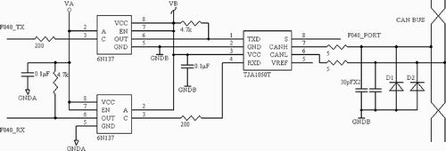
Figure 1 Intelligent node circuit
In Figure 1, the CAN signal receiving pin RX and the sending pin TX of C8051F040 are not directly connected to the RXD and TXD terminals of TJA1050T, but are connected via the high-speed optical coupler 6N137 to achieve electrical isolation of each node of the CAN bus. In order to achieve complete electrical isolation in the true sense, the VA and VB of the optical coupler part must be isolated through a DC-DC module or a switching power supply module with multiple isolated outputs. To prevent overcurrent shock, the CANH and CANL pins of TJA1050T are each connected to the bus through a 5Ω resistor. Two 30pF capacitors are connected in parallel between the CANH and CANL pins and the ground to filter out high-frequency interference on the bus. The lightning protection diodes D1 and D2 can protect against transient interference.
Pin 8 of TJA1050T is connected to a port of C8051F040 for mode selection. TJA1050T has high-speed mode and silent mode. It works normally in high-speed mode; in silent mode, the transmitter of TJA1050T is disabled and performs the listen-only function, which can be used to prevent network congestion caused by the loss of control of the CAN controller.
2 Intelligent node communication software design
2.1 CPU access mechanism to CAN registers
The CAN registers in C8051F040 are divided into three categories: CAN controller protocol registers, message object interface registers, and message processor registers. The three most important registers that control the main functions of CAN can be accessed directly like separate special function registers (SFRs). They are CAN control register, CAN test register and CAN status register. Some other registers are accessed through an indirect pointer mechanism.
The access method is to first enter the index number of the register to be accessed in the CAN0ADR register, and then access the CAN register through the CAN data registers (CAN0DATH and CAN0DATL). In order to speed up the access to the frequently accessed interface registers, there is an automatic addition function when accessing the index range 0x08~0x12 (interface register 1) and 0x20~0x2A (interface register 2). When the index number in CAN0ADR is within these two ranges, CAN0ADR can automatically add 1 each time CAN0DATL is read/written, pointing to the 16-bit word of the next CAN register. Of course, registers that use direct access can also be accessed using indirect access.
2.2 CPU access mechanism to message objects
The CAN module in C8051F040 provides a message mailbox (Message RAM) for CAN bus communication. The message mailbox contains 32 independent message objects (Message Object). The ID check code and acceptance filter code of each message object can be configured separately for message transmission and reception. To prevent conflicts between CPU access to the message mailbox and CAN message reception and transmission, the CPU does not directly access the message objects in the message mailbox, but accesses them through two groups of message object interface registers (IF1 and IF2). The
access method is that when the CPU wants to write a message object, it first sets the command mask register (CommandMask Register) of the register group to determine which fields of the message object are to be written, then sets the message buffer register, and finally writes the number of the message object to be written in the command request register (Command Request Register) to complete the write access to the message object. The
reading method is to first set the command mask register of the register group to determine which parts of the message object will be read out, and finally write the number of the message object to be read out in the command request register, so that the content of the message object to be read is transferred to the message buffer register in the message interface register group for the CPU to read. Generally, the message interface register group 1 is used for writing message objects, and the register group 2 is used for reading message objects.
2.3 Implementation of CAN controller communication software
In general, the most basic CAN bus node communication software includes three parts: CAN node initialization, message transmission, and message reception.
2.3.1 CAN node initialization
The initialization of intelligent nodes mainly includes the following parts: setting the CAN pin output mode, setting the baud rate parameters, initializing the message object, and setting the corresponding interrupt enable bit when receiving or sending interrupts are allowed. To enter the initialization state, the Init bit in the CAN control register must be set to 1. First, set the output mode of the CANTX port. By setting bit 7CTXOUT in the port cross switch register 3 (XBR3), select whether the CANTX port works in open drain or push-pull output mode. By default, the CANTX pin works in drain output mode. Then set the baud rate. Set the CCE bit to 1 and write the setting parameters to the corresponding registers, including the bit timing register and the BRP extension register (used at low communication rates).
Then set the message object through the message object interface register group (IFX). For example, by setting Dir, determine whether this is a send message object or a receive message object; set the Xtd bit to determine whether to use a standard frame or an extended frame, etc. If the receive interrupt or the send interrupt is allowed, the TxIE or RxIE bit must be set. For unused message objects, you can disable them by setting their MsgVal bit to 0. When the receive interrupt or the send interrupt is allowed, the corresponding interrupt enable bit must be set. These bits include the IE bit of the CAN control register and the ECAN0 bit of the EIE2 register. Finally, reset the Init and CCE bits to complete the setting. The flowchart of the initialization of the CAN node is shown in Figure 2.
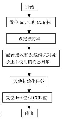
Figure 2 CAN node initialization flowchart
2. 3. 2 CAN node communication program in interrupt mode
Its general process is: first read the value of the interrupt register in the interrupt service subroutine to obtain the number of the message object that caused the interrupt; then determine whether it is a receive or send interrupt by judging whether RxOK or TxOk is set in the status register. If it is a sending interrupt, set the ClrIntPend bit and NewDat bit in the command mask register to 1, and clear the interrupt waiting bit and new data bit of the corresponding message object by reading the corresponding message object; if it is a receiving interrupt, read the corresponding data in the message object while clearing the above bits, and finally clear the corresponding bit in the status register. The flow chart is shown in Figure 3.
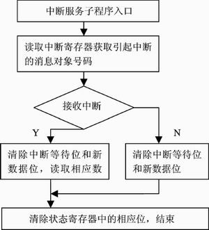
Figure 3 CAN node communication program in interrupt mode
2. 3. 3 CAN node message sending and receiving program in query mode
For the sending message object working in query mode, there are two ways to send messages. The
first method is to set the Txqst bit of its message request register to 1 to start sending a new message, and then query the TXOK bit in the status register to determine whether the message is successfully sent. After successful sending, clear the corresponding status flag bit. The flow chart is shown in Figure 4 (a).
The second method is to first determine whether the last message has been successfully transmitted by querying whether the corresponding Txqst bit in the send request register is 0. If it has been successfully transmitted, a new message can be started by setting the Txqst bit of its message request register to 1. The flowchart is shown in Figure 4 (b).
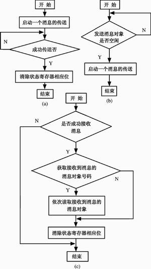
Figure 4 CAN node message sending and receiving program
For the receiving message object working in the query mode, first determine whether a message is successfully received by querying whether the RXOK in the status register is set, and then determine which message objects have successfully received the message by querying whether the new data bit (NewDat) set as the receiving message object in the new data register is 1, and then read the messages in these message objects in turn, and finally clear the RXOK bit of the status register. Note that if a message is successfully received, RXOK will be set regardless of whether it passes the acceptance filter. The flowchart of the CAN bus communication in the query mode is shown in Figure 4 (c). For the actual CAN bus measurement and control node, the general situation is to send in the query mode and receive in the interrupt mode.
Keywords:C8051F040
Reference address:Design of Intelligent Node in CAN Bus System Based on C8051F040
C8051F040 has a built-in CAN bus protocol controller. As long as the external bus driver chip and the appropriate anti-interference circuit are connected, a practical CAN bus intelligent measurement and control node can be easily established. This article uses the TJA1050T CAN bus driver of PH ILIP Company, and the hardware schematic diagram is shown in Figure 1.

Figure 1 Intelligent node circuit
In Figure 1, the CAN signal receiving pin RX and the sending pin TX of C8051F040 are not directly connected to the RXD and TXD terminals of TJA1050T, but are connected via the high-speed optical coupler 6N137 to achieve electrical isolation of each node of the CAN bus. In order to achieve complete electrical isolation in the true sense, the VA and VB of the optical coupler part must be isolated through a DC-DC module or a switching power supply module with multiple isolated outputs. To prevent overcurrent shock, the CANH and CANL pins of TJA1050T are each connected to the bus through a 5Ω resistor. Two 30pF capacitors are connected in parallel between the CANH and CANL pins and the ground to filter out high-frequency interference on the bus. The lightning protection diodes D1 and D2 can protect against transient interference.
Pin 8 of TJA1050T is connected to a port of C8051F040 for mode selection. TJA1050T has high-speed mode and silent mode. It works normally in high-speed mode; in silent mode, the transmitter of TJA1050T is disabled and performs the listen-only function, which can be used to prevent network congestion caused by the loss of control of the CAN controller.
2 Intelligent node communication software design
2.1 CPU access mechanism to CAN registers
The CAN registers in C8051F040 are divided into three categories: CAN controller protocol registers, message object interface registers, and message processor registers. The three most important registers that control the main functions of CAN can be accessed directly like separate special function registers (SFRs). They are CAN control register, CAN test register and CAN status register. Some other registers are accessed through an indirect pointer mechanism.
The access method is to first enter the index number of the register to be accessed in the CAN0ADR register, and then access the CAN register through the CAN data registers (CAN0DATH and CAN0DATL). In order to speed up the access to the frequently accessed interface registers, there is an automatic addition function when accessing the index range 0x08~0x12 (interface register 1) and 0x20~0x2A (interface register 2). When the index number in CAN0ADR is within these two ranges, CAN0ADR can automatically add 1 each time CAN0DATL is read/written, pointing to the 16-bit word of the next CAN register. Of course, registers that use direct access can also be accessed using indirect access.
2.2 CPU access mechanism to message objects
The CAN module in C8051F040 provides a message mailbox (Message RAM) for CAN bus communication. The message mailbox contains 32 independent message objects (Message Object). The ID check code and acceptance filter code of each message object can be configured separately for message transmission and reception. To prevent conflicts between CPU access to the message mailbox and CAN message reception and transmission, the CPU does not directly access the message objects in the message mailbox, but accesses them through two groups of message object interface registers (IF1 and IF2). The
access method is that when the CPU wants to write a message object, it first sets the command mask register (CommandMask Register) of the register group to determine which fields of the message object are to be written, then sets the message buffer register, and finally writes the number of the message object to be written in the command request register (Command Request Register) to complete the write access to the message object. The
reading method is to first set the command mask register of the register group to determine which parts of the message object will be read out, and finally write the number of the message object to be read out in the command request register, so that the content of the message object to be read is transferred to the message buffer register in the message interface register group for the CPU to read. Generally, the message interface register group 1 is used for writing message objects, and the register group 2 is used for reading message objects.
2.3 Implementation of CAN controller communication software
In general, the most basic CAN bus node communication software includes three parts: CAN node initialization, message transmission, and message reception.
2.3.1 CAN node initialization
The initialization of intelligent nodes mainly includes the following parts: setting the CAN pin output mode, setting the baud rate parameters, initializing the message object, and setting the corresponding interrupt enable bit when receiving or sending interrupts are allowed. To enter the initialization state, the Init bit in the CAN control register must be set to 1. First, set the output mode of the CANTX port. By setting bit 7CTXOUT in the port cross switch register 3 (XBR3), select whether the CANTX port works in open drain or push-pull output mode. By default, the CANTX pin works in drain output mode. Then set the baud rate. Set the CCE bit to 1 and write the setting parameters to the corresponding registers, including the bit timing register and the BRP extension register (used at low communication rates).
Then set the message object through the message object interface register group (IFX). For example, by setting Dir, determine whether this is a send message object or a receive message object; set the Xtd bit to determine whether to use a standard frame or an extended frame, etc. If the receive interrupt or the send interrupt is allowed, the TxIE or RxIE bit must be set. For unused message objects, you can disable them by setting their MsgVal bit to 0. When the receive interrupt or the send interrupt is allowed, the corresponding interrupt enable bit must be set. These bits include the IE bit of the CAN control register and the ECAN0 bit of the EIE2 register. Finally, reset the Init and CCE bits to complete the setting. The flowchart of the initialization of the CAN node is shown in Figure 2.

Figure 2 CAN node initialization flowchart
2. 3. 2 CAN node communication program in interrupt mode
Its general process is: first read the value of the interrupt register in the interrupt service subroutine to obtain the number of the message object that caused the interrupt; then determine whether it is a receive or send interrupt by judging whether RxOK or TxOk is set in the status register. If it is a sending interrupt, set the ClrIntPend bit and NewDat bit in the command mask register to 1, and clear the interrupt waiting bit and new data bit of the corresponding message object by reading the corresponding message object; if it is a receiving interrupt, read the corresponding data in the message object while clearing the above bits, and finally clear the corresponding bit in the status register. The flow chart is shown in Figure 3.

Figure 3 CAN node communication program in interrupt mode
2. 3. 3 CAN node message sending and receiving program in query mode
For the sending message object working in query mode, there are two ways to send messages. The
first method is to set the Txqst bit of its message request register to 1 to start sending a new message, and then query the TXOK bit in the status register to determine whether the message is successfully sent. After successful sending, clear the corresponding status flag bit. The flow chart is shown in Figure 4 (a).
The second method is to first determine whether the last message has been successfully transmitted by querying whether the corresponding Txqst bit in the send request register is 0. If it has been successfully transmitted, a new message can be started by setting the Txqst bit of its message request register to 1. The flowchart is shown in Figure 4 (b).

Figure 4 CAN node message sending and receiving program
For the receiving message object working in the query mode, first determine whether a message is successfully received by querying whether the RXOK in the status register is set, and then determine which message objects have successfully received the message by querying whether the new data bit (NewDat) set as the receiving message object in the new data register is 1, and then read the messages in these message objects in turn, and finally clear the RXOK bit of the status register. Note that if a message is successfully received, RXOK will be set regardless of whether it passes the acceptance filter. The flowchart of the CAN bus communication in the query mode is shown in Figure 4 (c). For the actual CAN bus measurement and control node, the general situation is to send in the query mode and receive in the interrupt mode.
Previous article:DC motor PWM closed-loop control experiment (complete C51 program)
Next article:Design of CAN bus intelligent node based on C8051F550
Latest Microcontroller Articles
He Limin Column
Microcontroller and Embedded Systems Bible
 Professor at Beihang University, dedicated to promoting microcontrollers and embedded systems for over 20 years.
MoreSelected Circuit Diagrams
MorePopular Articles
- Innolux's intelligent steer-by-wire solution makes cars smarter and safer
- 8051 MCU - Parity Check
- How to efficiently balance the sensitivity of tactile sensing interfaces
- What should I do if the servo motor shakes? What causes the servo motor to shake quickly?
- 【Brushless Motor】Analysis of three-phase BLDC motor and sharing of two popular development boards
- Midea Industrial Technology's subsidiaries Clou Electronics and Hekang New Energy jointly appeared at the Munich Battery Energy Storage Exhibition and Solar Energy Exhibition
- Guoxin Sichen | Application of ferroelectric memory PB85RS2MC in power battery management, with a capacity of 2M
- Analysis of common faults of frequency converter
- In a head-on competition with Qualcomm, what kind of cockpit products has Intel come up with?
- Dalian Rongke's all-vanadium liquid flow battery energy storage equipment industrialization project has entered the sprint stage before production
MoreDaily News
- Allegro MicroSystems Introduces Advanced Magnetic and Inductive Position Sensing Solutions at Electronica 2024
- Car key in the left hand, liveness detection radar in the right hand, UWB is imperative for cars!
- After a decade of rapid development, domestic CIS has entered the market
- Aegis Dagger Battery + Thor EM-i Super Hybrid, Geely New Energy has thrown out two "king bombs"
- A brief discussion on functional safety - fault, error, and failure
- In the smart car 2.0 cycle, these core industry chains are facing major opportunities!
- The United States and Japan are developing new batteries. CATL faces challenges? How should China's new energy battery industry respond?
- Murata launches high-precision 6-axis inertial sensor for automobiles
- Ford patents pre-charge alarm to help save costs and respond to emergencies
- New real-time microcontroller system from Texas Instruments enables smarter processing in automotive and industrial applications
Guess you like
- Constant voltage and constant current power supply design
- About the difference between CC1312R LAUNCHPAD versions
- About the signal input mode of the power amplifier
- My Journey of MCU Development (Part 1)
- How to understand the accuracy parameter (1.5% + 3) of the Fluke F17B+ multimeter?
- Inverting proportional operational amplifier circuit
- Upper computer displays waveform acquisition
- Evaluation Weekly Report 20211129: There are 4 days left for Anxinke NB-IoT and domestic FPGA applications, and the wireless charging mouse pad is waiting to be disassembled (Extra)
- EEWORLD University Hall----TI 77GHz millimeter wave radar product introduction and solution display
- TMS320F28377S LaunchPad XDS100 V2 driver cannot be installed

 Robot drive and control and application examples
 Robot drive and control and application examples


 京公网安备 11010802033920号