Data acquisition refers to the process of converting analog quantities such as temperature, pressure, voltage, current, displacement, and flow into digital quantities, and then storing, processing, displaying or printing them by a computer. The corresponding system is called a data acquisition system. This paper studies the problem that a single data acquisition instrument is difficult to collect and transmit various signals in real time at industrial sites due to the low CPU frequency and limited data processing capabilities of the current data acquisition instrument, and proposes a solution for hardware compression encoding of audio and video. The data acquisition instrument performs hardware compression encoding of the collected audio and video signals in MP3 and H.264 formats respectively, which greatly reduces the CPU resource occupation during data processing and the bandwidth occupation during data transmission, and solves the problem that portable data acquisition instruments are difficult to realize the integrated collection and transmission of multiple data at industrial sites. This data acquisition instrument integrates the acquisition, processing, and transmission of multiple signals at industrial sites, and has the advantages of high integration, small size, and strong scalability.

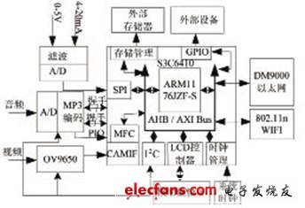
Figure 1 Data acquisition instrument structure diagram
Overall system design
According to the requirements of integrated data acquisition, the data acquisition instrument integrates the acquisition, processing and transmission of various data. Its composition is shown in Figure 1: The core processing chip of the data acquisition instrument adopts the 16-bit/32-bit RISC microprocessor S3C6410 launched by Samsung. It has a 64-bit/32-bit internal bus architecture, including multiple hardware accelerators. Its internal integrated multi-format codec (MFC) supports hardware encoding and decoding of multiple formats. In addition, S3C6410 includes many hardware peripherals (such as a camera interface, TFT24-bit true color LCD display controller, system manager, 4-channel UART, 32-channel DMA, general I/O port, IIS bus interface, IIC bus interface, USB host device, etc.), which greatly reduces the total cost of system design and improves system performance. The data acquisition part includes sensor output signal, audio and video signal acquisition. The CPU processes and judges the collected sensor signal. If the signal exceeds the normal value range, the data acquisition instrument will issue an alarm and control the external related devices to take action through the GPIO pin of S3C6410. The data collector has built-in large-capacity Nand Flash and SD card, which can store the signals collected on site for a long time. In terms of communication, the data collector uses the RT3070 wireless communication module produced by Ralink to communicate with the remote monitoring system. The RT3070 module is a high-speed WIFI module with a USB interface that supports the 802.11n protocol for embedded applications. The wireless communication rate can be as high as 150Mbps. Because the design of data display and storage circuits and serial port and Ethernet communication circuits has become very popular in ARM applications, this article will focus on the hardware design of the data acquisition part.
Sensor signal acquisition
The output signals of commonly used analog sensors in industry are 4mA-20mA current and 0-5V voltage. Since the signal transmission process is often distorted by other electromagnetic waves in the external environment, and sometimes the distortion is very serious, the data collector misjudges the on-site situation and directs the machine to malfunction, affecting the company's production efficiency, and sometimes even causing human life and huge property losses. Therefore, it is necessary to filter the collected signals first. In this design, the analog signal output by the industry is first filtered out of the high frequency by a filter and then sent to the A/D module for analog-to-digital conversion. The converted digital signal is read by the S3C6410 through the SPI interface.
Filter circuit design
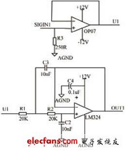
Filtering is essentially the process of extracting the information carried by the original signal from the signal that has been distorted and contaminated by noise. The filter circuit of the data collector is shown in Figure 2. Because the filtering and AD conversion signals are voltage signals, a 250Ω precision resistor and a voltage follower are added to the current input end. The current signal is first converted into a 1V-5V voltage signal through a precision resistor, and then enters the filter circuit after impedance matching through the voltage follower to filter out high-frequency interference. For voltage input, it directly enters the filter circuit for filtering. In the filter circuit, because the Butterworth response can maximize the passband flatness of the filter, it is particularly suitable for low-frequency applications. It is very important for maintaining the flatness of the gain, so this design uses a Butterworth second-order low-pass filter. The voltage signal is low-pass filtered by a second-order Butterworth filter composed of an op amp LM324. After filtering, the signal enters the A/D conversion module for A/D conversion. According to the characteristics of the Butterworth second-order filter, the cutoff frequency of the filter is:


Figure 2 Low-pass filter circuit
A/D conversion design
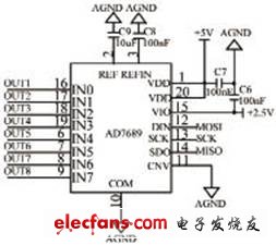
In data acquisition, it is often necessary to convert analog signals into digital signals that can be recognized by the processor so that the data acquisition instrument can process and transmit the signals. This requires the use of A/D conversion circuits. From the perspective of conversion principle, A/D converters mainly include parallel comparison type, successive approximation type and dual integral type. The parallel comparison type has a fast conversion speed, which can reach tens of nanoseconds, but it is expensive and is generally not used unless necessary; the dual integral type A/D converter has a longer conversion time, generally reaching 40ms~50ms; the successive approximation type has a higher conversion speed, which can reach several microseconds, and the price is moderate. This design uses the AD7689 chip produced by ADI to perform A/D conversion on the filtered voltage signal. AD7689 is an 8-channel, 16-bit resolution, no missing code, charge redistribution successive approximation analog-to-digital converter (ADC) powered by a single power supply. AD7689 uses a simple SPI interface to write configuration registers and output conversion results.
Audio acquisition design
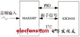
One of the main features of embedded products is that CPU resources are limited. In order to reduce the burden of CPU in data processing and reduce the bandwidth required for data transmission, this design performs hardware compression encoding on the collected audio and video data. The MAS3587 chip produced by Micronas Semiconductor Design and Manufacturing Company is used in audio acquisition processing. The chip integrates preamplifier and A/D conversion modules, supports analog and digital serial and parallel input and output, and has MPEG1/2 layer3 format encoding and MPEG1/2 layer2 and layer3 format decoding functions. The chip contains a headphone driver module, and the analog output signal can directly drive the headphone without amplification. The audio acquisition circuit is shown in Figure 4. After receiving the analog signal input, MAS3587 first converts the analog signal into a digital signal through the A/D part of the chip, and then sends the digital signal output after A/D conversion to the chip's built-in MP3 compression encoding module to complete the MP3 format encoding. In Figure 4, S3C6410 initializes the MAS3587 chip through the I2C bus, reads the audio data encoded in MP3 format through the handshake signal line and the parallel data line, and stores and transmits the data.

Figure 3 A/D conversion circuit

Figure 4 Schematic diagram of audio acquisition
Other module designs
Video Capture
In video acquisition, because the S3C6410 processor integrates multimedia codec (MFC), supports MPEG4/H.263/H.264 codec and VC1 decoding, it can provide real-time video conferencing and TV output in NTSC and PAL formats. In addition, the S3C6410 integrates the CameraIF interface, supports ITU RBT-601/656YCBCr 8-bit standard, and the maximum input size is 4096×4096 pixels. This design makes full use of the on-chip resources of S3C6410 to complete video acquisition and hardware compression encoding. Video acquisition directly connects to the OV9650 camera through the CameraIF interface of S3C6410 to collect live video data, and then uses the MFC module built into the chip to perform hardware compression encoding of the collected video signal in H.264 format.
WIFI communication
The wireless communication with the host computer greatly reduces the environmental restrictions when collecting data. Wireless data collection has the advantages of convenient installation, flexible use, and easy expansion. The data collection location can be changed at any time, and it is also very convenient to upload data. In order to meet the requirements of real-time transmission of large amounts of data, the data collector uses the 802.11n protocol to communicate with the host computer. The 802.11n protocol is a wireless transmission standard protocol of the Wi-Fi Alliance after 802.11a/b/g. It has faster data transmission speed and stronger signal stability than 802.11a/b/g. The purpose of the protocol is to achieve high-bandwidth, high-quality WLAN services, so that the wireless LAN can reach the performance level of Ethernet. Here, we use the RALINK RT3070 high-speed wireless network card. The network card driver supports embedded operating systems such as Windows CE and Linux, and is compatible with IEEE802.11b/g/n standards. It has the advantages of small size, stable signal, and fast data transmission speed (up to 150Mbps).
Conclusion
This paper takes the integrated acquisition of industrial field sensors and audio and video signals as the research content, and performs hardware compression encoding on the audio and video signals with huge data volume, saving the resource occupation and data transmission bandwidth in the CPU data processing process. Taking advantage of the high integration and fast data processing speed of the S3C6410 processor, a data acquisition instrument hardware platform integrating the acquisition, processing and transmission of multiple physical quantities is designed. The acquisition instrument has the advantages of small size, high integration, stable signal and flexible use. It can be used for data acquisition and monitoring in underground mines, power stations, factories and other places, and has broad application prospects.
Previous article:Design of smart home data acquisition system based on S3C2410
Next article:STM32 ADC configuration
- Popular Resources
- Popular amplifiers
 Professor at Beihang University, dedicated to promoting microcontrollers and embedded systems for over 20 years.
- Innolux's intelligent steer-by-wire solution makes cars smarter and safer
- 8051 MCU - Parity Check
- How to efficiently balance the sensitivity of tactile sensing interfaces
- What should I do if the servo motor shakes? What causes the servo motor to shake quickly?
- 【Brushless Motor】Analysis of three-phase BLDC motor and sharing of two popular development boards
- Midea Industrial Technology's subsidiaries Clou Electronics and Hekang New Energy jointly appeared at the Munich Battery Energy Storage Exhibition and Solar Energy Exhibition
- Guoxin Sichen | Application of ferroelectric memory PB85RS2MC in power battery management, with a capacity of 2M
- Analysis of common faults of frequency converter
- In a head-on competition with Qualcomm, what kind of cockpit products has Intel come up with?
- Dalian Rongke's all-vanadium liquid flow battery energy storage equipment industrialization project has entered the sprint stage before production
- Allegro MicroSystems Introduces Advanced Magnetic and Inductive Position Sensing Solutions at Electronica 2024
- Car key in the left hand, liveness detection radar in the right hand, UWB is imperative for cars!
- After a decade of rapid development, domestic CIS has entered the market
- Aegis Dagger Battery + Thor EM-i Super Hybrid, Geely New Energy has thrown out two "king bombs"
- A brief discussion on functional safety - fault, error, and failure
- In the smart car 2.0 cycle, these core industry chains are facing major opportunities!
- The United States and Japan are developing new batteries. CATL faces challenges? How should China's new energy battery industry respond?
- Murata launches high-precision 6-axis inertial sensor for automobiles
- Ford patents pre-charge alarm to help save costs and respond to emergencies
- New real-time microcontroller system from Texas Instruments enables smarter processing in automotive and industrial applications
- TI Power
- New support for STM32WB55 in MicrPython
- Useful Information|Selected from TI CC3200-LAUNCHXL Evaluation Report
- 100k bridge
- [Zero-knowledge ESP8266 tutorial] Quick Start 6- Make your creations sound
- Remove a chip from a DDR3 1600Mhz 4G memory stick and then put it back together
- 【RT-Thread Reading Notes】7. RT-Thread Study Chapters 8-12 Reading Notes
- EEWORLD University ---- Introduction to Linux Kernel Programming
- ATSAM MCU
- Share your TouchGFX design and win an STM32F750 development board. Come on board!

 TLC254CDRG4


 京公网安备 11010802033920号