1. Detailed explanation of hardware design
1) A/D conversion principle
This is accomplished through the three steps of sampling, quantization, and encoding. First, the input analog voltage signal is sampled, and after the sampling is completed, the holding time begins.
During this period of time, the sampled voltage is converted into a digital quantity, and the conversion result is given in a certain coding form, and then the next sampling begins.
Sampling must satisfy the sampling theorem, that is, the sampling frequency fs must be greater than the frequency of the highest frequency component fimax of the input signal. Generally, fs = (2~3)fimax,
2) Types of A/D converters
There are two types, direct A/D converter and indirect A/D converter.
Direct A/D converters include parallel comparison A/D converters and feedback comparison A/D converters.
The indirect A/D converter includes a voltage-time conversion type (VT conversion type) and a voltage-frequency conversion type (VF conversion type).
a. Parallel comparison A/D converter schematic diagram:
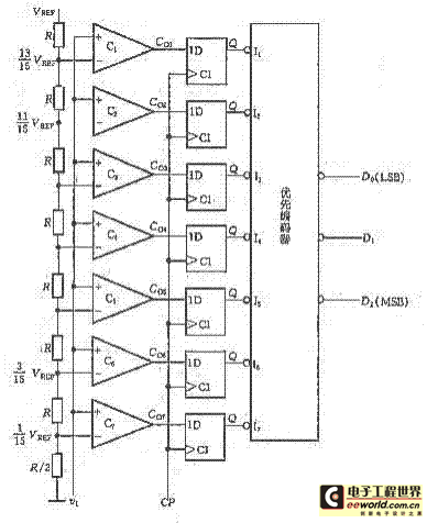
a.1 Principle Description
The three-bit parallel comparator A/D converter consists of a voltage comparator, a register and a code converter. The reference voltage Vref is divided by a resistor chain.
Get 7 comparison levels from 1/15Vref to 13/15Vref, with the unit of quantization being 2/15Vref. Then add the analog voltage to be input simultaneously
The other input of each comparator is compared with these 7 comparison references.
a.2 Product Introduction
AD company's AD
9012 (8-bit), AD9002 (8-bit), AD9020 (10-bit).
a.3 Features
Since the conversion is parallel, the conversion time is only limited by the delay time of the comparator, trigger and encoding circuit, so the conversion speed is fast; (advantage)
As the resolution increases, the number of components increases exponentially. (Disadvantages)
When using this parallel A/D conversion circuit with registers, there is no need to add a sample-and-hold circuit because the comparator and register are
It also has a sample-and-hold function. (Advantage)
b. Feedback Comparator A/D Converter
b.1 Principle Description
Take a digital quantity and add it to the D/A converter, then get a corresponding output analog voltage, and compare this analog voltage with the input analog voltage
The signals are compared. If the two are not equal, the digital value taken is adjusted until the two analog voltages are equal. The final digital value taken is
This is the desired conversion result.
b.2 Implementation plan
Counting type and successive comparison type
The counting converter is mainly composed of comparator C, D/A converter, counter, pulse source, control gate G and output register.
The principle is to use the reset signal to set the counter to 0 before the conversion starts, and the conversion signal should stay in the state of Vl=0, then the gate G is blocked and the counter
Does not work. The timer adds a full 0 signal to the D/A converter, so the analog voltage V0 output by the D/A converter is 0. If Vi is a positive voltage signal,
The output voltage of the comparator is 1. Compare all the digits of DA in the same way. Since the digits in the counter keep changing during the conversion process,
Therefore, it is not appropriate to use the state of the counter directly as the output signal. For this reason, an output register is set at the output end. After each conversion is completed,
The falling edge of the conversion control signal places the number output by the counter into the output register, and the state of the register is used as the final output signal.
The problem with this method is that the conversion speed is slow and the conversion time is long. It is suitable for occasions where the conversion speed requirement is not high.
Successive approximation converter logic circuit diagram
C is a voltage comparator. When Vi>=Vo, the comparator output is 0; otherwise, the output is 1. The three triggers FFa, FFb, and FFc form a three-digit digital
The register, flip-flops FF1~FF5 and gate circuits G1~G9 constitute a control logic circuit.
The time required for a successive approximation A/D converter to complete a conversion is related to the number of bits and the clock pulse frequency. The fewer the number of bits, the higher the clock frequency.
The shorter the time required for conversion. This A/D converter has the characteristics of fast conversion speed and high precision. Its products mainly include
ADC0804/0808/0809 series (8 bits), AD575 (10 bits), and AD574A (12 bits).
c. Voltage-time conversion type (vt conversion type)
The principle is to convert the input analog voltage signal into a time width signal proportional to it, and then use the fixed frequency clock in this time width.
Pulse counting, the counting result is a digital signal proportional to the input analog voltage.
d. Voltage-frequency conversion type (VF conversion type)
The principle is to convert the input analog voltage signal into a frequency signal proportional to it, and then obtain the frequency at a fixed time interval.
The signal is counted, and the result is a digital quantity proportional to the input analog voltage.
3) A/D converter parameters
a. Resolution
Describe the A/D converter's ability to resolve input signals.
The resolution of the A/D converter is expressed in the number of bits of the output binary number. The more bits the output has, the smaller the quantization unit is and the higher the resolution is.
b. Conversion error
Indicates the difference between the actual digital output of the A/D converter and the theoretical output digital quantity.
c. Conversion accuracy
The maximum quantization error of the A/D converter and the accuracy of the analog part are combined.
d. Conversion time
The time it takes for the A/D converter to obtain a stable digital signal from the time the conversion control signal arrives.
4) ADC0804 Description
a. Pin diagram
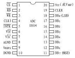
Vin(+), Vin(-) - Two analog signal input terminals, used to accept unipolar, bipolar and differential input signals.
DB7~DB0 - Digital signal output port with three-state characteristics.
AGND - Analog signal ground
DGND - Digital signal ground
CLK - Clock signal input
CLKR - The external resistor terminal of the internal clock generator. When combined with the CLK terminal, the chip can generate clock pulses with a frequency of 1/(1.1RC)
/CS - Chip select signal input terminal, low level is valid. Once valid, it indicates that the A/D converter is selected and can start working.
/WR - Write signal input, low level starts A/D conversion.
/RD - Read signal input, low level output is valid.
/INTR - A/D conversion end signal, a low level indicates that the conversion is completed.
Vref/2 - Reference level input, determines the quantization unit.
Vcc - Chip power 5V input.
b. Conversion timing diagram
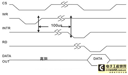
CS is low first, and /WR is then set low. After at least tw(/WR)L time, /WR is pulled high. As the A/D converter is started, and after
After (1 to 8 A/D clock cycles + internal Tc) time, the analog-to-digital conversion is completed, the conversion result is stored in the data latch, and INTR automatically changes to
Low level notifies the microcontroller that the conversion is complete.
When reading data, after /INTR becomes low, set /CS low first, then set /RD low. After /RD is set low for at least tACC time,
The data on the digital output port reaches a stable state. At this time, directly reading the digital output port data can obtain the converted digital signal.
After the data is received, /RD is pulled high immediately, and then /CS is pulled high. /INTR changes automatically. When /RD is set low for tR1 time, /INTR is automatically pulled high.
We don't have to think about interfering.
The above timing diagram is the timing diagram of ADC0804 starting once and reading data once. When we want to convert and read data continuously, there is no
It is necessary to set /CS low and then pull it high every time, because /CS is the chip select signal. Setting it low means that the chip can be operated or is in a normal working state, so
When writing a program, only /CS needs to be set low at the beginning. Later, when you want to start the conversion and read the data, you only need to operate /WR and /RD.
2. Detailed explanation of programming
1. Use a single-chip microcomputer to control ADC0804 for analog-to-digital conversion
Program features:
When the potentiometer Re2 next to the A/D on the experimental board is turned, the digital value after A/D conversion is dynamically displayed in decimal form in the first three digits of the digital tube (the value after 8-bit A/D conversion varies from 0 to 255).
Program source code:
#include
#include
#define uchar unsigned char
#define uint unsigned int
sbit dula = P2^6;
sbit wela = P2^7;
sbit adwr = P3^6;
sbit adrd = P3^7;
uchar code table[] = {
0x3f,0x06,0x5b,0x4f,
0x66,0x6d,0x7d,0x07,
0x7f,0x6f,0x77,0x7c,
0x39,0x5e,0x79,0x71
};
void delayms(uint);
void display(uint);
void main()
{
uchar i, adval;
uint num;
wela = 1;
P0 = 0x7f;
wela = 0;
while (1)
{
adwr = 1;
_nop_();
adwr = 0;
_nop_();
adwr = 1;
for (i = 10; i > 0; i--)
display(num);
P1 = 0xff;
adrd = 1;
_nop_();
adrd = 0;
_nop_();
adval = P1;
adrd = 1;
num = adval;
}
}
void delayms(uint xms)
{
uint i, j;
for (i = xms; i > 0; i--)
for (j = 110; j > 0; j--)
;
}
void display(uint num)
{
dula = 1;
P0 = table[num / 100];
dula = 0;
P0 = 0xff;
wela = 1;
P0 = 0x7e;
wela = 0;
delayms(5);
dula = 1;
P0 = table[num % 100 / 10];
dula = 0;
P0 = 0xff;
wela = 1;
P0 = 0x7d;
wela = 0;
delayms(5);
dula = 1;
P0 = table[num % 100 % 10];
dula = 0;
P0 = 0xff;
wela = 1;
P0 = 0x7b;
wela = 0;
delayms(5);
}
Program Summary:
1) After entering the main program, first set the highest position of the output port of the U2 latch to a low level, in order to set the /CS chip select terminal of the ADC0804 connected to it to a low level.
Set it low to select, because the data is read continuously, so select it once and don't worry about it later. At the same time, please note that in the future, whenever you operate the U2 latch terminal
Do not change the /CS terminal of A/D. In the digital tube display program, when sending the bit selection signal, always keep the highest bit of U2 latch at low level.
In the above example, “P0=0x7e;P0=0x7d;P0=0x7b;” in the digital tube display part of the program is the same.
2) After entering the while(1) loop, A/D conversion is started first, and the _nop_() in it is equivalent to a delay of one machine cycle.
3) After starting the A/D conversion, the result is sent to the digital tube for display immediately before the conversion result is read. The purpose of this is to
Leave some time,
4) If the digital tube digits do not change when you turn the potentiometer, the digits will be refreshed only after resetting or powering on again.
The reason is that there is not enough time. The solution is to increase a in for(a=10;a>0;a--).


 MATLAB and FPGA implementation of wireless communication
 Modern Electronic Technology Training Course (Edited by Yao Youfeng)
 Operational Amplifier Practical Reference Handbook (Edited by Liu Changsheng, Zhao Mingying, Liu Xu, etc.)
 A Complete Illustrated Guide to Operational Amplifier Applications (Written by Wang Zhenhong)
 Professor at Beihang University, dedicated to promoting microcontrollers and embedded systems for over 20 years.
 MATLAB and FPGA implementation of wireless communication


 京公网安备 11010802033920号