I. Introduction
During the mining, construction and use of tunnels, the deformation of tunnel surrounding rock is the most direct and reliable reflection of the surrounding rock stress distribution, overall mechanical morphology changes and stable state. The measurement of surrounding rock clearance displacement is an important link in the tunnel construction process and an important basis for judging the stability of surrounding rock and guiding construction. Timely monitoring, analysis and prediction of tunnel surrounding rock deformation has become a very important task in tunnel construction to ensure construction safety, prevent accidents and reasonably determine tunnel support.
There are two main methods for measuring displacement of tunnel surrounding rock in traditional ways: one is to arrange the measurement section during the construction process, and use various mechanical or mechanical-electronic convergence meters to measure at regular intervals; the other is to use a tunnel section meter to measure the section to be measured at fixed points at regular intervals. The shortcomings of both methods are:
(1) Inability to monitor in real time: that is, the deformation of the section to be measured cannot be monitored at any time, and therefore, the abnormal changes in the tunnel surrounding rock during the construction process cannot be reflected in a timely manner.
(2) Great interference to construction: Since deformation measurement requires either a ruler or the installation of a cross-section instrument, it has a great impact on construction work, especially transportation operations.
(3) Dangerous measurement work: In places that are difficult for personnel to access, in order to obtain measurement data, personnel have to frequently approach dangerous spaces, which poses a greater threat to the safety of personnel and instruments.
(4) High measurement cost: The same section needs to be measured repeatedly, and the measurement process is complicated, requires many people, and takes a long time, resulting in high measurement costs.
(5) Unreliable measurement data: The main reasons for unreliable measurement data are insufficient measurement accuracy of electronic and mechanical instruments and errors caused when processing measurement data.
Since the above five main shortcomings limit the traditional tunnel monitoring technology, this system uses PIC32 processor to build a railway tunnel monitoring system, which has the advantages of high integration, fast processing speed, real-time monitoring, etc. The PIC32 processor has an operating frequency of up to 80MHZ, 32-bit processing width, 32K RAM, and 10-bit, 500ksps A/D, which can reduce the peripheral devices of the product, enhance system stability, and reduce system costs.
2. Overall solution design
Schematic diagram of the principle of monitoring surrounding rock displacement during railway tunnel construction using laser beam and CCD 2-1. It consists of four parts: semiconductor laser light source and beam conversion transmission, CCD sensor, data acquisition, collection, processing and transmission module, bracket (fixed CCD) light sensor and laser light source relative position, including micro-adjustment bracket, etc.). Figure 2-2 is a picture of the installation on the construction site, and Figure 2-3 is a simulation platform built in the laboratory.
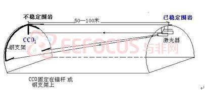
Figure 2-1 Schematic diagram of railway tunnel monitoring principle

Figure 2-2 Setting up a monitoring platform on the construction site
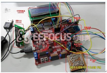
Figure 2-3 Experimental simulation platform
The design block diagram of the entire system is shown below. PIC32MX460F512L is used as the core processor. The entire system is divided into data acquisition, data display, data storage, and data communication.
The data acquisition part is: drive the linear array CCD TCD1501 through the RA interface; because the linear array CCD outputs an analog signal, it needs to be converted into a digital signal that can be processed by the MCU through the ADC interface, and the current spot position is calculated; use the I2C interface to connect the temperature sensor LM75 to obtain the current temperature data; use the RTCC interface to obtain the current real-time clock and calendar. Data display part: use the PMP interface to drive the character LCD1602 to display the current time, temperature, and spot position information. Data storage part: use the SPI interface to drive the commonly used miniSD card, and use the popular file operating system FatFS to store time, temperature, and spot position data. Data communication part: use the USART interface to transfer data to the host computer through serial communication, and use the graphical programming software LabVIEW for programming.
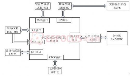
Figure 2-4 Block diagram of the entire system
3. Introduction of each module
3.1 Linear CCD TCD1501
3.1.1 Working Principle of Linear Array CCD
CCD is a semiconductor device consisting of a series of adjacent MOS (metal-oxide-semiconductor) storage units. Under external light conditions, it can generate charges and store them in MOS storage units. The amount of charges generated is proportional to the intensity of the incident light and the exposure time. Driven by a certain external voltage, the charges stored in the CCD can be moved one by one in sequence, and an output voltage proportional to the stored charge is generated at the output end through the output amplifier. A working cycle of CCD is divided into two stages: light integration stage and charge transfer stage. The light integration stage realizes the accumulation of photocharges, while at the same time outputting the charges in the previous frame shift register and clearing the invalid charges in the pixel potential well; the charge transfer stage realizes the transfer of photocharges to the shift register. The photosensitive array and shift register of CCD are separated. The pixel receives external light source to generate charges, and the transfer gate controls the transfer of photogenerated signal charges to the shift register. Generally, the signal transfer time is much shorter than the light integration time. The transfer signal controls the transfer gate, the transfer gate is closed, and the photosensitive array collects the light signal. At this time, the photosensitive array and the shift register are in a blocking state, and no charge transfer occurs. [page]
3.1.2 Introduction to Toshiba TCD-1501
TCD-1501 is a linear array CCD produced by Toshiba Semiconductor with 5000 effective pixels, single 12V power supply, extremely high sensitivity, pixel size of 7um×7um, typical clock pulse frequency of 1MHz, and maximum up to 12MHz. The actual picture is shown in the figure:

Figure 3-1 Physical picture of TCD1501
3.1.3 PIC32 drives TCD1501
The timing diagram of TCD1501 is shown in Figure 2-2, and the schematic diagram constructed using Altium Designer is shown in Figure 2-3. The five ports RA0 to RA5 of PIC32 are used to output the timing of Figure 2-2. Since the conversion range of the ADC inside the PIC is 0 to 3.3, the output result is processed by the two-stage proportional differential amplifier circuit LM358. The first stage subtracts CCD_OS from CCD_DOS, and the second stage forms a voltage follower, using potentiometer R5 to proportionally abbreviate the output voltage.

Figure 3-2 TCD1501 timing diagram
3.1.3 MPLAP software simulation and experimental test
Use MPLAB software to write the driver software, and select MPLAB SIM in the DEBUG selection for software simulation, as shown in Figure 3-4. Then use the Tektronix oscilloscope TDS1012 to detect the CCD output voltage. It can be seen that the drive is successful and a periodic waveform is output. In one of the waveforms, the high voltage part indicates that light is detected here, and the low voltage part indicates that there is no light.
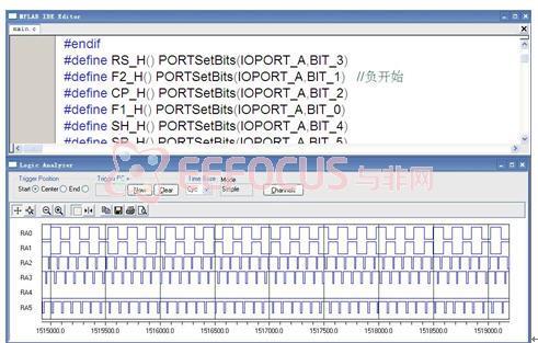
Figure 3-4 Software simulation using MPLAB
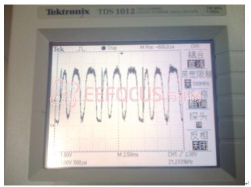
Figure 3-5 Using Tektronix oscilloscope TDS1012 to detect CCD output voltage
3.2 Character LCD1602
3.2.1 Introduction to LCD1602
LCD1602 is a commonly used industrial-grade character LCD that can display 16×2, or 32 characters at the same time. The figure below shows the physical picture and pin definition. The character generator memory (CGROM) inside the module has stored 160 different dot matrix character graphics, including Arabic numerals, uppercase and lowercase English letters, commonly used symbols, and Japanese kana, etc. Each character has a fixed code.

Figure 3-6 LCD1602 physical diagram and pin definition
|
Pinout |
symbol |
Function Description |
|
1 |
VSS |
General grounding |
|
2 |
VDD |
Connect to power supply (+5V) |
|
3 |
V0 |
The contrast adjustment terminal of the LCD display has the weakest contrast when connected to the positive power supply and the highest contrast when connected to the ground power supply (when the contrast is too high, "ghost images" will be produced. The contrast can be adjusted through a 10K potentiometer during use). |
|
4 |
RS |
RS is the register selection. When the high level is 1, the data register is selected, and when the low level is 0, the instruction register is selected. |
|
5 |
R/W |
R/W is the read/write signal line. A high level (1) is used for read operation, and a low level (0) is used for write operation. |
|
6 |
EN |
The E (or EN) terminal is the enable terminal, and the falling edge enables. |
|
7 |
DB0 |
The bottom 4 bits are tri-state, bidirectional data bus bit 0 (lowest bit) |
|
8 |
DB1 |
Bottom 4 bits tri-state, bidirectional data bus 1 bit |
|
9 |
DB2 |
Bottom 4 bits tri-state, bidirectional data bus 2 bits |
|
10 |
DB3 |
Bottom 4 bits tri-state, bidirectional data bus 3 bits |
|
11 |
DB4 |
High 4 bits tri-state, bidirectional data bus 4 bits |
|
12 |
DB5 |
High 4 bits tri-state, bidirectional data bus 5 bits |
|
13 |
DB6 |
High 4 bits tri-state, bidirectional data bus 6 bits |
|
14 |
DB7 |
High 4 bits tri-state, bidirectional data bus 7 bits (highest bit) (also busy flang) |
|
15 |
BLA |
Backlight power positive |
|
16 |
BLK |
Backlight power negative terminal |
3.2.2 Introduction to Parallel Master Interface PWP
The Parallel Master Port (PMP) is an 8-bit/16-bit parallel I/O module that is dedicated to communicating with a variety of parallel devices such as communication peripherals, LCDs, external storage devices, and microcontrollers. Due to the diversity of parallel peripheral interfaces, the PMP module is highly configurable. [page]
Key features of the PMP module include:
• Up to 16 programmable address lines
• Up to 2 chip select lines
• Programmable strobe options
• Separate read and write strobes, or
• Read/Write strobe with enable strobe
• Address auto-increment/auto-decrement
• Programmable address/data multiplexing
• Programmable control signal polarity
• Support for legacy parallel slave port
• Supports Enhanced Parallel Slave Port
• Address support
• 4-byte deep auto-increment buffer
• Schmitt trigger or TTL input buffer
3.2.3 Configuring PMP for LCD Module
From the above, we know about LCD1602. Although we can manually access the pins of PORTE and PORTD to control the I/0 signal to realize the bus timing, the parallel master interface PMP provided by PIC32 can free the microcontroller from the tedious task of controlling slow peripheral devices. Figure 3-7 is the connection diagram of using PMP interface with LCD1602, and Figure 3-8 is driving the LCD to display a line of "EEFOCUS GOOD" characters.
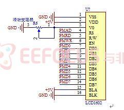
Figure 3-7 Connection diagram of PMP interface and LCD1602
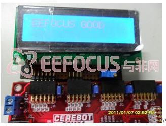
Figure 3-8 Driving the LCD to display a line of "EEFOCUS GOOD" characters
2.3 Serial communication COM
Serial interface is abbreviated as serial port, also known as serial communication interface (usually refers to COM interface), which is an expansion interface using serial communication. Due to its simple configuration, it is widely used to transfer data to computers. Since there is no serial port module on the development board and we have not applied for a serial port module, we soldered a serial port module ourselves according to the schematic diagram of Figure 3-9, using the serial port 2 interface of PIC32 and the MAX232 chip, as shown in the figure.

Figure 3-9 PIC32 serial port 2 interface and MAX232 chip circuit connection
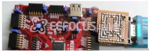
Figure 3-10 Serial port module physical picture
3.4 Temperature sensor LM75A
3.4.1 Introduction to LM75A
LM75A is a high-speed I2C interface temperature sensor that can directly convert temperature into digital signals within the temperature range of -55 to +125, and achieve an accuracy of 0.125. PIC32 can directly read the data in its internal registers through the I2C bus, and can operate 4 data registers through I2C to set different working modes. LM75A has 3 optional logic address pins, so that 8 devices can be connected to the same bus at the same time without address conflicts.
3.4.2 LM75A Implementation
The connection between LM75A and PIC32 is in the form of I2C bus, as shown in Figure 3-11. Pull-up resistors are required on the bus because the I2C bus must be idle or not busy before communication begins. This means that all devices on the bus must release the SCL and SDA lines. The SCL and SDA lines are pulled high by the pull-up resistors of the bus. The pull-up resistors are about 10K. The actual connection diagram is shown in the figure.
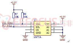
Figure 3-11 Connection diagram between PIC32's I2C1 interface and LM75A
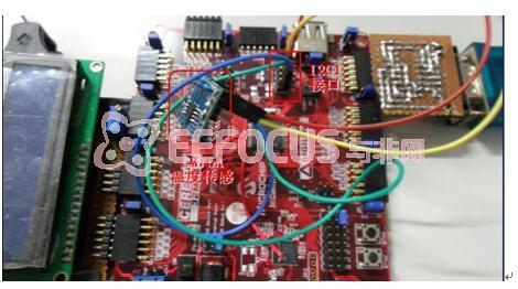
Figure 3-12 LM75A and I2C1 interface physical continuity diagram
3.5 Real-time clock and calendar
Since the collected data needs to be marked with time, the PIC32 device provides a hardware real-time clock and calendar (RTCC). This module provides real-time clock and calendar functions. RTCC is designed for applications that need to maintain accurate time for a long time without or with minimal CPU intervention. The module is optimized for low-power use to extend battery life while tracking time. The RTCC module has a 100-year clock and calendar that can automatically detect leap years. The clock range is from 00:00:00 (midnight) on January 1, 2000 to 23:59:59 on December 31, 2099. The hours are provided in a 24-hour (military time) format. The clock provides a time granularity of one second, and the user can see a half-second time interval. An external 32.768KHZ low-speed crystal oscillator is required. Since the development board does not have a soldered crystal oscillator, we soldered a crystal oscillator and a chip capacitor ourselves to speed up the crystal oscillator start-up speed. The following figure shows the current time and date on the LCD using the RTCC module. The first line is: Current time is:, and the second line is: 16-46-25 03-07, indicating that the current time is March 7, 16:46:25.
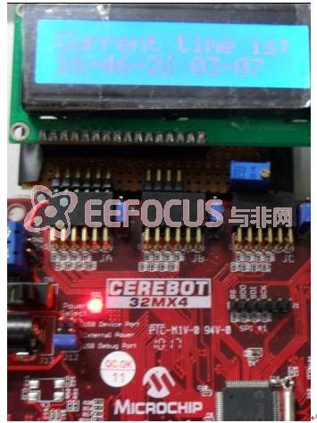
Figure 3-13 Using the RTCC module to display the current time
3.6 Data storage miniSD
This section introduces the miniSD memory card, how to connect it to the SPI module of PIC32, and introduces the commonly used FATFS file operating system.
3.6.1 Introduction to miniSD
Mini-SD card is a smaller memory card that is more suitable for small mobile phones and is developed based on the Flash used in digital cameras, PDAs, etc. (full name: Memory Card). Although the size and interface shape of mini-SD card are different from those of the original SD card, the electrical standards such as the interface are the same to ensure compatibility. By inserting the mini-SD card into a dedicated adapter, the mini-SD card can be read and written through the original SD card slot. However, it does not have a write-proof lock function like the SD card. [page]
3.6.2 Connecting miniSD to PIC32
As shown in Figure 2-13, the SPI1 interface is used to connect to the miniSD card. Figure 2-14 is the actual connection diagram.
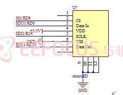
Figure 3-14 Using SPI1 interface to connect to miniSD card
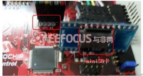
Figure 3-15 Physical connection diagram
3.6.3 Fatfs file operating system
FatFs is a general file system module for implementing FAT file systems in small embedded systems. FatFs is written in ANSI C and is therefore not hardware platform dependent. It can be embedded in cheap microcontrollers such as 8051, PIC, AVR, SH, Z80, H8, ARM, etc. without any modification. Features: FAT12, FAT16 and FAT32. Multiple volumes (physical drives and partitions). Two partitioning schemes: FDISK and Super-floppy. Multiple configuration options: Long file name support. Optional code pages, including DBCS (DBCS stands for Double Byte Char Systems) Multitasking support Read-only, minimized API, buffer configuration and other application program interfaces. Because the FatFs module is completely separated from the disk I/O layer, the following functions are needed to implement the underlying physical disk read and write and get the current time. The underlying disk I/O module is not part of FatFs and must be provided by the user.
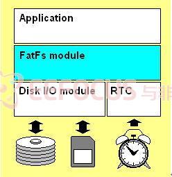
Figure 3-16 FatFs file operating system model
3.7 Host Computer LabVIEW
3.7.1 Introduction to LabVIEW
LabVIEW (Laboratory Virtual Instrument Engineering Workbench) is a graphical programming language development environment that is different from traditional text programming languages. It uses graphical structures and block diagrams to build program codes. It is a virtual instrument development platform developed by National Instruments NI, and is also the most popular, most powerful, and fastest-growing graphical programming language, commonly known as the G language.
Traditional text programming languages, such as C, Java, VB, etc., have a common feature: using letters to form words, using words to express certain data operations; using words to form statements, using statements to express operations such as assignment and calculation of certain data. These computer languages refer to human natural language and are highly abstract languages. Its advantage is high efficiency, and it can express complex functions with short sentences; its disadvantage is that the text is not intuitive enough and not easy to learn. Developers need to spend a lot of time learning and memorizing its keywords, programming syntax rules, etc., and text languages often cannot provide information to readers intuitively, and they need to read the entire code program to understand its meaning. At present, many high-level languages, such as VB and VC, introduce visual design methods in program interface design, and directly use the mouse to select and adjust the program interface, so that the effect of the program can be directly seen when it is running. Although they use graphical methods in interface design, the functions of the program still need to be realized through text programming. Compared with the above programming languages, LabVIEW not only uses graphical programming methods in program design, but also uses graphical programming methods when writing program code and realizing program functions. In a LabVIEW program, you see not lines of text, but lines and connections of various small graphic blocks. Since graphics are more intuitive than text, LabVIEW is easier to learn than other programming languages, allowing developers to allocate more time to data processing and algorithm analysis, improving programming efficiency, reducing hardware costs, and shortening system development cycles.
3.7.2 Host computer program
Use the VISA module in LabVIEW to implement serial communication. The program interface is as follows. By selecting the serial port number and the baud rate of communication, the CCD waveform data can be displayed on the panel, which is consistent with the oscilloscope acquisition data in Figure 3-5.
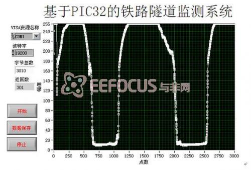
Figure 3-17 Host computer interface
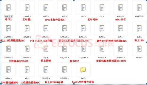
Four modular software design
Previous article:Intelligent network based on TCP/IP network protocol and zigbee wireless sensor network implemented on PIC32
Next article:Multi-layer pipe string electromagnetic flaw detection and logging system based on single chip microcomputer
Recommended ReadingLatest update time:2024-11-16 20:44

- Popular Resources
- Popular amplifiers
 Professor at Beihang University, dedicated to promoting microcontrollers and embedded systems for over 20 years.
- Innolux's intelligent steer-by-wire solution makes cars smarter and safer
- 8051 MCU - Parity Check
- How to efficiently balance the sensitivity of tactile sensing interfaces
- What should I do if the servo motor shakes? What causes the servo motor to shake quickly?
- 【Brushless Motor】Analysis of three-phase BLDC motor and sharing of two popular development boards
- Midea Industrial Technology's subsidiaries Clou Electronics and Hekang New Energy jointly appeared at the Munich Battery Energy Storage Exhibition and Solar Energy Exhibition
- Guoxin Sichen | Application of ferroelectric memory PB85RS2MC in power battery management, with a capacity of 2M
- Analysis of common faults of frequency converter
- In a head-on competition with Qualcomm, what kind of cockpit products has Intel come up with?
- Dalian Rongke's all-vanadium liquid flow battery energy storage equipment industrialization project has entered the sprint stage before production
- Allegro MicroSystems Introduces Advanced Magnetic and Inductive Position Sensing Solutions at Electronica 2024
- Car key in the left hand, liveness detection radar in the right hand, UWB is imperative for cars!
- After a decade of rapid development, domestic CIS has entered the market
- Aegis Dagger Battery + Thor EM-i Super Hybrid, Geely New Energy has thrown out two "king bombs"
- A brief discussion on functional safety - fault, error, and failure
- In the smart car 2.0 cycle, these core industry chains are facing major opportunities!
- The United States and Japan are developing new batteries. CATL faces challenges? How should China's new energy battery industry respond?
- Murata launches high-precision 6-axis inertial sensor for automobiles
- Ford patents pre-charge alarm to help save costs and respond to emergencies
- New real-time microcontroller system from Texas Instruments enables smarter processing in automotive and industrial applications
- 5 major drawbacks of using UWB for indoor positioning, a full summary of practical information
- After the zstack coordinator is powered off and restarted, the node cannot access the network?
- High-performance lossless data decompression IP based on LZO
- Newcomer Report
- Benefits of IoT
- 【NUCLEO-WL55JC2 Review】Summary
- Blackberry tablet palybook account number and password problem help
- [GD32E503 Review] Part 2: Environment Setup
- TL TMS320C6748 Development Board User Manual
- RL leading phase shift circuit, RL lagging phase shift circuit

 Design of touch-controlled intelligent home control system
 MCU Principles and Interface Technology C51 Programming (Edited by Zhang Yigang)
 Example interpretation of 51 single chip microcomputer complete learning and application


 京公网安备 11010802033920号