O Introduction
In the past two decades, power electronics technology has developed rapidly and has been widely used in the fields of electricity, metallurgy, chemical industry, coal, communication, home appliances, etc. Most power electronic devices are connected to the power grid through rectifiers. The classic rectifier is a nonlinear circuit composed of diodes or thyristors, which will generate a large amount of current harmonics and reactive power in the power grid, polluting the power grid and becoming a power hazard. In the mid-to-late 1980s, the active power factor correction technology of switching power supplies attracted the attention of many scholars at home and abroad, and many special studies were carried out and a lot of results were achieved.
Active power factor correction technology adds a DC/DC switching converter between the rectifier and the filter capacitor. Among various single-phase PFC circuit topologies, Boost power factor correction circuits are widely used due to their simple main circuit structure, high conversion efficiency, and easy control strategy implementation. High frequency can reduce the volume and weight of active power factor correction circuits and improve the power density of the circuit. In order to enable the circuit to operate efficiently at high frequencies, soft switching technology of active power factor correction circuits has become an important research direction.
This paper classifies the soft switching technology of single-phase Boost active power factor correction circuit and analyzes the topology, working mode and working characteristics of each type of circuit.
l Zero Voltage Switching (ZVS) PWM Power Factor Correction Circuit
ZVS工作方式是指利用谐振现象及有关器件的箝位作用,使开关变换器中开关管的电压在开启或关断过程中维持为零。
The circuit in Figure 1 is a ZVS power factor correction circuit, also known as an extended cycle quasi-resonant power factor correction circuit. When the auxiliary switch S1 is turned on, the inductor Lr suppresses the reverse recovery of the diode Dr. The inductor Lr and the capacitor Cf resonate until the current flowing through the switch S1 drops to the input current. After the switch S2 is turned on, the inductor Lr and the capacitor Cf resonate again until the current flowing through the switch S1 is 0, and the voltage across the capacitor Cr is Vo, so that the switches S1 and S2 achieve ZV-ZCS shutdown. The disadvantage of the circuit is that the current stress of the switch is relatively large.

2 Zero Voltage Transition (ZVT) PWM Power Factor Correction Circuit
In the ZVT working mode, the resonant network topology is connected in parallel with the main circuit. The conduction loss and switching loss of the zero-conversion PWM power factor correction circuit are very small, and it can achieve zero switching characteristics without increasing the current or voltage stress of the switch, which is suitable for higher voltage and high power converters.
The circuit shown in Figure 2 is a traditional ZVT circuit. The inductor Lr resonates with the parasitic capacitance of the main switch S1 to turn on its parasitic diode, and the switch S1 is turned on in ZVS; at the same time, the inductor Lr suppresses the reverse recovery of the diode D1, and the diode D2 provides a release loop for the energy in the inductor Lr.
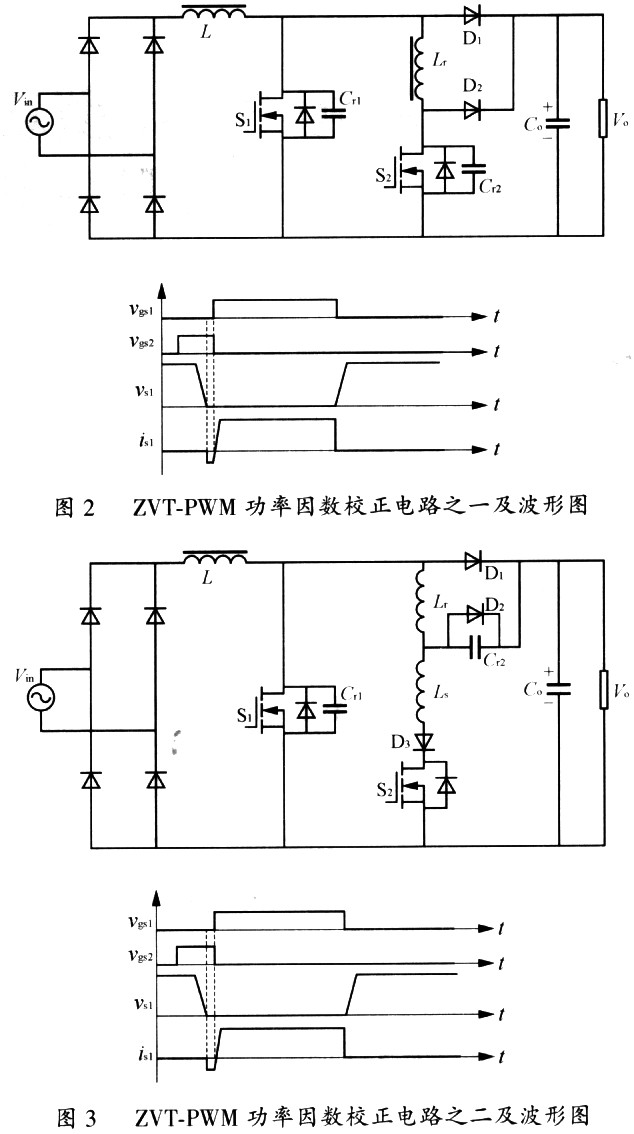
The advantages of this circuit are that the main switch is turned on with ZVS, the reverse recovery of the diode D1 is suppressed, and the circuit structure is simple; the disadvantage is that the auxiliary switch is turned on with hard switching.
Figure 3 shows an improved circuit of the traditional ZVT circuit, and its switching timing, voltage and current waveforms of the switch are the same as those of Figure 2. The improvement is that a diode D3 is connected in series in the inductor loop to eliminate the parasitic oscillation between the parasitic capacitance of the boost diode D1 and the inductor Lr; a capacitor is connected in parallel at both ends of the diode D2 to reduce the turn-off loss of the switch S2, which can improve the efficiency of the circuit.
The shortcoming of the circuit is that the auxiliary switch of the improved circuit is still hard-on.
The main switch S1 in the circuit shown in Figure 4 is turned on by ZVS. Its turn-on process is slightly different from the above two circuits. When the resonant inductor Lsn2 and the capacitor Csn1 resonate with the parasitic capacitance of the switch S1 until the voltage across the switch S1 is zero, the switch S1 is turned on. Csn1 and Csn2 can improve the turn-off process of the switches S1 and S2 and reduce the turn-off loss. The inductor Lsn2 suppresses the reverse recovery of the diode D. The diodes Db and Dc provide an energy release loop for the inductor Lsn2.
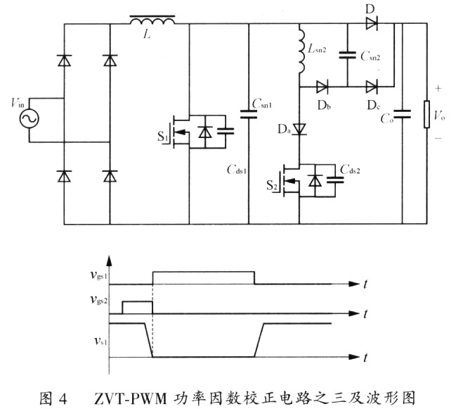
The shortcoming of the circuit is that the auxiliary switch S2 is hard turned on.
The circuit of Figure 5 is an improvement on the circuit of Figure 4. As shown in the waveform, before the main switch S1 is turned on, its parasitic diode is already turned on, and the switch S1 achieves ZVS turn-on; after the switch S1 is turned on, due to the effect of the coupling inductor, the current flowing through Lx is rapidly reduced to near zero, and the auxiliary switch S2 achieves ZCS turn-off; the capacitor Cr reduces the turn-off loss of the circuit.

The disadvantage of the circuit is that the auxiliary switch S2 is hard-on, and the circuit structure and working mode are relatively complicated.
The circuit shown in Figure 6 is another improved circuit of the traditional ZVT circuit. Before the main switch S1 is turned on, its parasitic diode is already turned on, and the switch S1 can achieve ZVS turn-on; after the switch S1 is turned on, due to the effect of the coupling inductor, the current flowing through the auxiliary switch S2 drops rapidly to near zero, and the switch S2 is clamped at a very low voltage by the breakdown diode Ds, and the switch S2 achieves ZCS turn-off.

The disadvantage of the circuit is that the auxiliary switch is hard-on, and the structure and working mode of the circuit are relatively complicated.
The circuit structure shown in Figure 7 is quite different from the above ZVT structure. After the main switch S1 is turned off, the diode D is turned on, and the capacitor Cc is discharged through the coupled inductor N2. The parasitic diode of switch S2 is turned on to achieve ZVS turn-on; after switch S2 is turned off, the parasitic diode of switch S1 is turned on to achieve ZVS turn-on. At the same time, the coupled inductor N1 suppresses the reverse recovery of the diode D, and the coupled inductor N2 provides a release loop for the energy in N1.

The advantages of this circuit are that both switches are turned on by ZVS, the reverse recovery of diode D is suppressed, and the circuit structure is simple. The disadvantages are that both switches are turned off by hard switching, and the voltage stress of auxiliary switch S2 is large.
The circuit shown in Figure 8 is a new type of ZVT active power factor correction circuit. Before the auxiliary switch S2 is turned on, the voltage across the capacitor Cr is negative. After S2 is turned on, the inductor Lr resonates with the capacitors Cs and Cr, causing the parasitic diode of the main switch S1 to turn on and achieve ZVS turn-on; when the current flowing through the switch S1 changes from negative to positive, the inductor Lr resonates with the capacitors Cb and Cr, the diode D5 turns on, and the switch S2 achieves ZV-ZCS turn-off.

电路优点在于主开关S1实现了ZVS开通,辅助开关S2实现了ZV.ZCS关断,二极管D1的反向恢复得到抑制,以上几点都可以显著提高电路效率。电路不足之处是辅助开关硬开通,主开关电流应力比较大。
The circuit structure and working mode of the circuit shown in Figure 9 are quite special. After the main switch S1 is turned off, its parasitic capacitance is charged to the output voltage Vo by constant current, providing ZV-ZCS turn-off for the auxiliary switch S2, at which time diodes D. and D4 are turned on; after the switch S2 is turned off, the inductor L resonates with the parasitic capacitance of the switch S2 until the voltage across the switch S2 is equal to Vo, and the diode D3 is turned on; when the current flowing through the inductor L decreases to zero, the inductor L resonates with the parasitic capacitance of the switches S1 and S2. When the resonance ends, the voltage across the switches S1 and S2 and the current flowing through the two switches are both zero, and the switches S1 and S2 achieve ZV-ZCS turn-on.
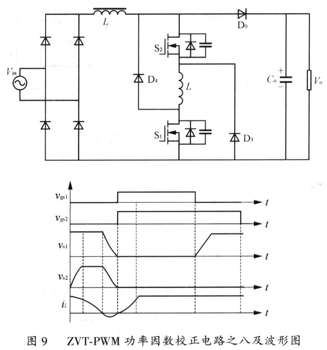
The advantages of this circuit are that switches S1 and S2 realize ZV-ZCS turn-on, switch S1 realizes ZVS turn-off, the reverse recovery of the diode is suppressed, the switch voltage and current stress is small, and the circuit structure is simple. The disadvantage is that the inductor L always has current flowing through it, resulting in a large circulating current in the current, which will increase the conduction loss.
3 Zero Current Switching (ZCS) PWM Power Factor Correction Circuit
ZCS工作方式是指利用谐振现象及有关器件的箝位作用,使开关变换器中开关管电流在开启或关断过程中维持为零。
It can be seen from the circuit and waveform diagram of Figure 10 that the main switch S1 is turned on first, and the current passing through the switch S1 gradually increases to the input current value. At this time, the diodes D1 and D2 are turned off, and the capacitor Cr is reversely charged to Vo; after the auxiliary switch S2 is turned on, the capacitor Cr resonates with Lr2. When the voltage across the capacitor Cr drops to zero, the diode D1 is turned on, and the capacitor Cr resonates with the inductors Lrl and Lr2 until the switches S1 and S2 anti-parallel diodes are turned on, and the two switches are turned off to achieve ZCS.

The advantage of this circuit is that switches S1 and S2 both achieve ZCS shutdown, and the reverse recovery of the two diodes is suppressed; the disadvantage is that the two switches are hard-on, and the resonant circuit of capacitor Cr and inductor Lr2 and inductor Lr1 and Lr2 must pass through the output end, which will increase the voltage fluctuation at the output end.
The circuit of Figure 11 is an improvement on the circuit of Figure 10. The working mode and waveform of the improved circuit are basically the same as those of the circuit of Figure 10. The circuit of Figure 11 changes the capacitor connected in parallel with the two ends of the diode to be connected in parallel with the switch S2 and the inductor Lr2. In this way, the resonant circuit will not include the output end and will not cause fluctuations in the output end voltage. Its disadvantage is still that the two switches are hard switched on.

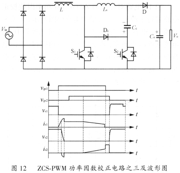
The biggest difference between the circuit in Figure 12 and the above two circuits is that it realizes the ZVS turn-on of one switch. As shown in the waveform diagram, the main switch S1 is turned on, the inductor Ls suppresses the reverse recovery of the diode D, the inductor Ls resonates with the capacitor Cr, and the switch S2 anti-parallel diode is turned on, providing ZVS turn-on for the switch S2; the capacitor Cc and the inductor Ls continue to resonate, and when the current flowing through the capacitor Cc is reversed, the switch S1 anti-parallel diode is turned on, realizing ZCS turn-off.
[page]
The advantage of this circuit is that the main switch S1 realizes ZCS shutdown and the auxiliary switch S2 realizes ZVS switch-on, so this circuit is also called ZV-ZCS circuit. The disadvantage of the circuit is the hard shutdown of the auxiliary switch S2.
4 Zero Current Transition (ZCT) PWM Power Factor Correction Circuit
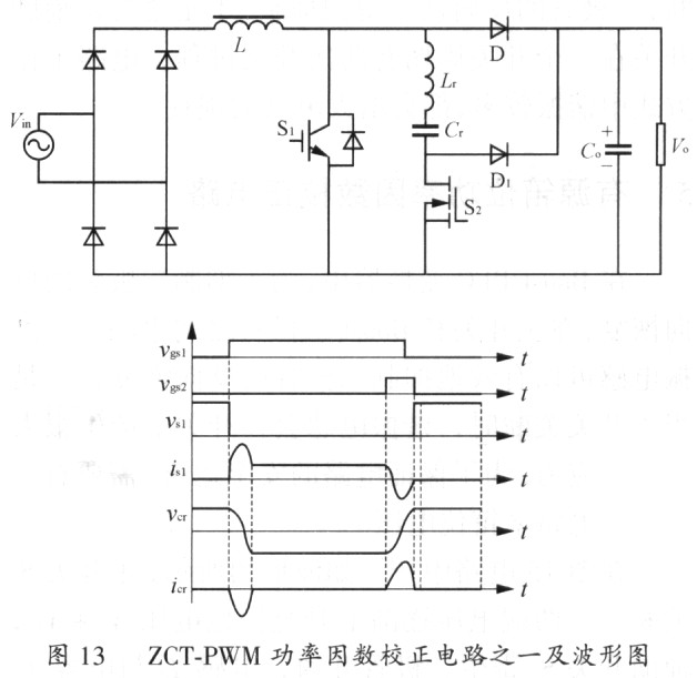
The circuit in Figure 13 is a traditional zero current conversion power factor correction circuit. As shown in Figure 13, when the auxiliary switch S2 is turned on, the capacitor Cr resonates with the inductor Lr, and the anti-parallel diode of the main switch S1 is turned on to achieve ZCS shutdown; after the anti-parallel diode of the switch S1 is turned off, the switch S2 is turned off, and the diode D1 is turned on to provide an energy release circuit for the inductor Lr.
The advantage of this circuit is that the ZCS shutdown of the main switch S1 is realized and the circuit structure is simple. The disadvantage is that the auxiliary switch is hard switched on and off, the reverse recovery of the diode is not suppressed, and the current stress of the main switch is large.
The circuit in Figure 14 improves the traditional ZCT-PWM power factor correction circuit. As shown in the waveform in Figure 14, when switch S2 is turned on, capacitor Cr and inductor Lr resonate, the current flowing through diode D1 gradually decreases to zero, and its reverse recovery is suppressed; after the resonant current is commutated, switch S2 reverse-parallel diode is turned on, and ZCS shutdown is achieved; after switch S2 is turned on, capacitor Cr and inductor lr resonate, switch S1 reverse-parallel diode is turned on, and ZCS shutdown is achieved.
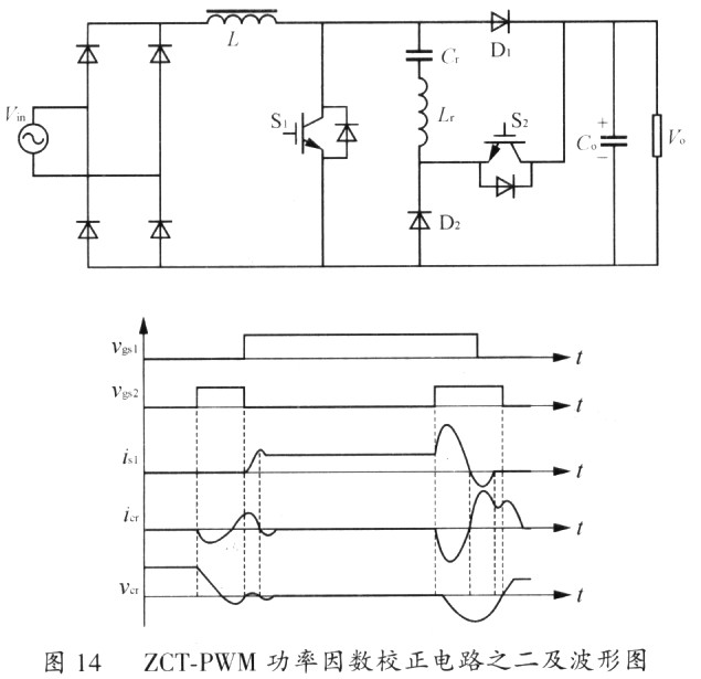
The advantage of this circuit is that the ZCS turn-off of switches S1 and S2 is achieved, and the reverse recovery of the diode is suppressed; the disadvantage is that the auxiliary switch has two switching processes in one switching cycle, and there are more resonances in the circuit working mode, which will increase the loss of the circuit.
5 有源箝位功率因数校正电路
在Boost PFC变换器中,为了抑制二极管的反向恢复,在主开关和Boost二极管之间串联一个谐振电感可以有效地抑制二极管的反向恢复,但是当主开关关断时,谐振电感会在开关上产生很大的电压应力,为了保证电路的安全运行,需要有一个箝位电路来箝位电压。
在图15电路中,如波形图所示,主开关Sl关断后,两端电压逐渐上升至箝位电压Vo+Vcc;辅助开关S2寄生二极管开通,电感Lr与电容Cc谐振,开关S2实现ZCS开通;开关S2关断后,二极管Db开通,电感Lr与开关S1寄生电容谐振至开关S1寄生二极管开通,开关S1一实现ZVS开通。电路增加二极管Dc是为了消除二极管Db结电容与电感Lr的谐振。

The advantage of the circuit is that the zvs of the main switch and the auxiliary switch are turned on, and the reverse recovery of the diode Db is suppressed; the disadvantage is that the switches S1 and S2 are both hard-off.
复合有源箝位功率因数校正电路对有源箝位功率因数校正电路的改进主要体现在电路拓扑和控制时序两个方面:将二极管D2放在箝位电路外以消除二极管D2结电容与电感Lr的寄生振荡;如图16所示时序可以保证开关S1、S2与二极管D2在任一时刻只有两个器件导通,另一个器件被箝位在Vo+Vcco主开关S1关断后,电感Lr与开关S2寄生电容谐振使寄生二极管导通实现ZVS开通;开关S2关断后,电感Lr与开关S1、S2寄生电容谐振使开关S1寄生二极管导通实现ZVS开通。

此电路的优点在于两个开关均实现了ZVS开通,二极管的反向恢复得到抑制,电路结构简单;不足之处是开关与二极管的电压应力较大。针对这一不足,提出了最小电压复合有源箝位电路,如图17所示,该电路将电感Lr与辅助开关S2位置进行了交换,开关时序不变,这样,开关S1、S2、二极管D2任两者导通时,另一个被箝位在Voo。该电路波形与复合有源箝位功率因数校正电路相似,具有它的优点。

6 Power factor correction circuit with lossless absorption circuit
6.1 Passive lossless absorption circuit
In soft switching technology, the passive lossless absorption circuit does not add additional active devices, but only uses passive components to suppress the reverse recovery of the diode and reduce the turn-on and turn-off losses of the switching device. Therefore, it has the advantages of low circuit cost and simple control.
In the circuit of Figure 18, after the switch S is turned off, the voltage across its ends is gradually charged to Vo, the diodes Do and Dc are turned on, the current flowing through the diode Dr gradually increases, and the current flowing through the diodes Do and Dc gradually decreases until the diode Doj is turned off. When the switch S is turned on again, the reverse recovery of the diode will not affect the increase in switching loss.
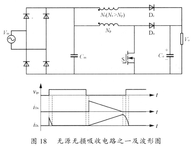
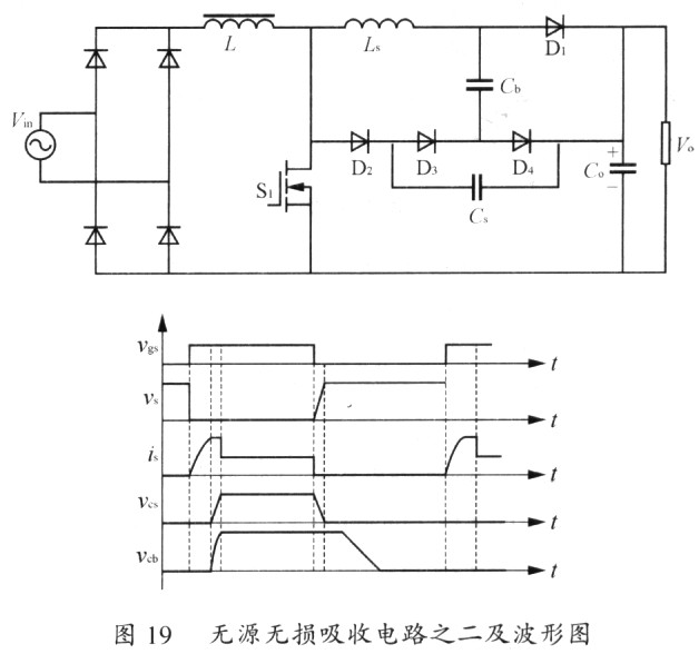
The circuit of Figure 18 uses a coupled inductor to prevent the reverse recovery of the diode from affecting the turn-on of the switch. The circuit of Figure 19 uses an inductor to suppress the effect of the reverse recovery of the diode on the turn-on process of the switch, and then uses passive devices to release the energy in the inductor.
The disadvantage of this circuit is that the circuit structure and working process are relatively complicated.
6.2 Active Lossless Absorption Circuit
The circuit in Figure 20 suppresses the reverse recovery of the diode by adding an inductor to the circuit and then releasing the energy in the inductor. As shown in Figure 20, the main switch S1 is turned on first, the inductor Ls suppresses the reverse recovery of the diode D, the inductor Ls resonates with the parasitic capacitance of the switch S2 to discharge it until the parasitic diode of the switch is turned on, and the switch S2 is turned on to achieve ZVS.
The advantage of this circuit is that the circuit structure is simple, the reverse recovery of the diode can be effectively suppressed, and the auxiliary switch can achieve ZVS turn-on.

7 Conclusion
In summary, various types of soft-switching power factor correction circuits have the ability to suppress diode reverse recovery, achieve soft turning on or off of the switch tube, reduce converter losses, and thus increase switching frequency, reduce the volume and weight of magnetic components, and improve converter power density.
Previous article:An Active Clamp Flyback Converter Achieving ZVS in the Full Load Range
Next article:Research on a New Topology of Dual Forward DC/DC Converter
Recommended ReadingLatest update time:2024-11-16 21:42

- Popular Resources
- Popular amplifiers
-
 Design of interleaved parallel Boost switching power supply module_Zuo Guanfang
 -
 Design of low power Boost switching power converter_Zeng Dong
 -
 Power Electronics Technology 3rd Edition (Edited by He Yikang and Pan Zaiping)
 -
 Research on AC chopper power converter and its control technology (by Jin Nan and Cui Guangzhao)
- MathWorks and NXP Collaborate to Launch Model-Based Design Toolbox for Battery Management Systems
- STMicroelectronics' advanced galvanically isolated gate driver STGAP3S provides flexible protection for IGBTs and SiC MOSFETs
- New diaphragm-free solid-state lithium battery technology is launched: the distance between the positive and negative electrodes is less than 0.000001 meters
- [“Source” Observe the Autumn Series] Application and testing of the next generation of semiconductor gallium oxide device photodetectors
- 采用自主设计封装,绝缘电阻显著提高!ROHM开发出更高电压xEV系统的SiC肖特基势垒二极管
- Will GaN replace SiC? PI's disruptive 1700V InnoMux2 is here to demonstrate
- From Isolation to the Third and a Half Generation: Understanding Naxinwei's Gate Driver IC in One Article
- The appeal of 48 V technology: importance, benefits and key factors in system-level applications
- Important breakthrough in recycling of used lithium-ion batteries
- Innolux's intelligent steer-by-wire solution makes cars smarter and safer
- 8051 MCU - Parity Check
- How to efficiently balance the sensitivity of tactile sensing interfaces
- What should I do if the servo motor shakes? What causes the servo motor to shake quickly?
- 【Brushless Motor】Analysis of three-phase BLDC motor and sharing of two popular development boards
- Midea Industrial Technology's subsidiaries Clou Electronics and Hekang New Energy jointly appeared at the Munich Battery Energy Storage Exhibition and Solar Energy Exhibition
- Guoxin Sichen | Application of ferroelectric memory PB85RS2MC in power battery management, with a capacity of 2M
- Analysis of common faults of frequency converter
- In a head-on competition with Qualcomm, what kind of cockpit products has Intel come up with?
- Dalian Rongke's all-vanadium liquid flow battery energy storage equipment industrialization project has entered the sprint stage before production
- Allegro MicroSystems Introduces Advanced Magnetic and Inductive Position Sensing Solutions at Electronica 2024
- Car key in the left hand, liveness detection radar in the right hand, UWB is imperative for cars!
- After a decade of rapid development, domestic CIS has entered the market
- Aegis Dagger Battery + Thor EM-i Super Hybrid, Geely New Energy has thrown out two "king bombs"
- A brief discussion on functional safety - fault, error, and failure
- In the smart car 2.0 cycle, these core industry chains are facing major opportunities!
- The United States and Japan are developing new batteries. CATL faces challenges? How should China's new energy battery industry respond?
- Murata launches high-precision 6-axis inertial sensor for automobiles
- Ford patents pre-charge alarm to help save costs and respond to emergencies
- New real-time microcontroller system from Texas Instruments enables smarter processing in automotive and industrial applications
- Request a free DCM evaluation sample
- Breaking News | Tesla's self-developed new battery heat ignites the market
- MicroPython adds support for NXP i.MX.RT
- There is a problem with the graphics output of the TDA2030 typical circuit. . .
- [MM32 eMiniBoard Review] In-depth understanding of HID
- PT100 temperature measurement circuit
- How do uboot multiple device trees adapt to the board and find the corresponding device tree?
- LSM6DSO32, an inertial module that supports MIPI I3C interface
- [FreeRTOS check-in station 6 opened] Experiment: serial port background printing, closing time August 29
- [RVB2601 Creative Application Development] 2. Try to control the onboard RGB

 Design of interleaved parallel Boost switching power supply module_Zuo Guanfang


 京公网安备 11010802033920号