TOPSwitch-FX series single-chip power integrated circuits are widely used in various general and special switching power supplies, standby power supplies, and switching power supply modules.
1. 12V, 30W switching power supply with external current limiting
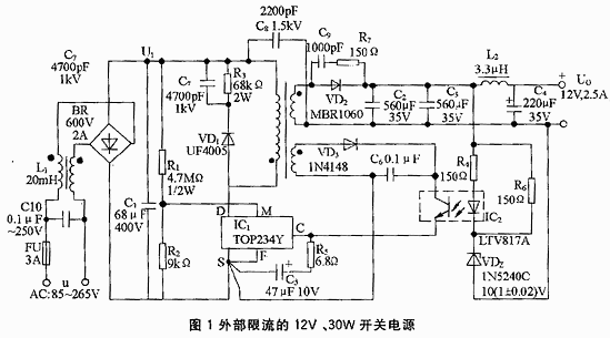
The circuit of a 12V, 30W high-efficiency switching power supply composed of TOP234Y is shown in Figure 1. Its AC input voltage range is AC85~265V, and the power efficiency can reach 80% when fully loaded. The AC voltage u passes through the electromagnetic interference (EMI) filter (C10, L1) and the input rectifier filter (BR, C1) in turn to obtain the DC high voltage UI. UI is connected to the M terminal after being divided by R1 and R2, which can reduce the limit current as UI increases. R1 can provide a voltage feedforward signal, and when UI is high, it can automatically reduce the maximum duty cycle to reduce the output ripple. R2 is the current limit setting resistor, and the set Ilimit≈0.7Ilimit=0.7×1.5A=1.05A is slightly higher than the peak current Ip value at low voltage input. The coefficient is taken as 0.7 here because the maximum continuous output power Pom=45W of TOP234Y under wide input range, while the actual output power P'om=30M, that is, P'om/Pom=30/45=0.67≈0.7. This design method allows the high-frequency transformer to use a smaller core, reduce the power consumption of TOP234Y by increasing the primary inductance Lp, and prevent magnetic saturation. In addition, due to the use of voltage feedforward technology to reduce Dmax, the switching power supply can work normally even if the input voltage UI and the primary induction voltage UOR are high. It allows the use of low-cost R, C, VD type drain clamp circuit (R3, C7, VD1) to replace the more expensive TVS (transient voltage suppressor) and VD type clamp circuit to absorb the spike voltage generated by the leakage inductance of the high-frequency transformer when TOP234Y is turned off, and protect the drain.

After the secondary voltage is rectified and filtered by VD2, C2, C3, L2 and C4, a regulated output of +12V and 2.5A is obtained. To reduce the loss of the rectifier tube, VD2 uses the MBR1060 10A/60V Schottky diode. C9 and R7 are connected in parallel at both ends of VD2 to prevent VD2 from self-oscillating (ringing) under high-frequency switching conditions. When the switching power supply is unloaded, TOPSwitch-FX can further reduce the maximum output duty cycle by skipping cycles, making Dmax <1.5%. Therefore, there is no need to connect a dummy load at the output end, which can also reduce the power consumption in no-load or standby states.
The power supply uses an optocoupler feedback circuit with a voltage regulator. IC2 is an LTV817A linear optocoupler. VDZ uses a 1N5240C voltage regulator, and its stable voltage Uz=10 (1±0.02) V. The forward voltage drop UF≈1V of the LED in the optocoupler. The output voltage is determined by the following formula:
Uo=Uz+UF+UR4
The voltage stabilization principle is analyzed as follows: When Uo↑ due to some reason, Uo>U2+UF+UR4, the error voltage Ur'=Uo-(Uz+UF+UR4) generated will make the IF of LED↑, and after the optical coupler, the IE of the receiving tube↑, so that the control end current Ic↑, and the duty cycle D↓, resulting in Uo↓, thus achieving the purpose of voltage stabilization. Conversely, Uo↓→IF↓→IE↓→Ic↓→D↑→Uo↑, which also plays a role in voltage stabilization.
The typical value of the stable current of 1N5240C is 20mA. When R4=150Ω, it can only supply 6.7mA of current. Further increasing the resistance value will be limited by the LED working current IF (usually 3.5~7mA). For this reason, the resistor R6 provides another 13.3mA working current, so that the stable current Iz of VDz=3.7mA+13.3mA=20mA, and its voltage regulation characteristics are also improved. After the feedback winding voltage is rectified and filtered by VD3 and C6, a 12V feedback voltage is generated, which is passed through IC2 to provide bias voltage to the control end of TOP234Y. C5 is a bypass capacitor, which also forms a compensation circuit of the control loop with R5.

2. 35W set-top box switch circuit with multiple outputs
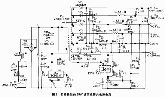
The 35W set-top box switching power supply circuit with 5 outputs is shown in Figure 2. The 5 voltages are: Uo1 (+30V, 100mA), Uo2 (+18V, 550mA), Uo3 (+5V, 2.5A), Uo4 (+3.3V, 3A), Uo5 (-5V, 100mA). Among them, +5V and +3.3V are the main outputs, and the rest are auxiliary outputs. When the AC input voltage u=220(1±0.15)V, the total output power reaches 38.5W; if a wide range voltage input (u=85~265V AC) is used, the total output power is reduced to 25W, which can be used as a switching power supply in set-top boxes (Set-top Box), video recorders (VCR), video camcorders (CVCR) and DVDs. The power supply uses three ICs: TOP233Y (IC1), optocoupler LTV817A (IC2), and adjustable precision shunt regulator TL431C (IC3). In order to reduce the volume of the high-frequency transformer and enhance the degree of magnetic field coupling, the secondary winding adopts a stacked winding method. The absorption loop composed of R4 and C14 can reduce the interference of radio frequency noise on video equipment such as televisions. If necessary, the switching frequency selection terminal (F) can be connected to the control terminal (C) to select the half-frequency mode to further reduce the sensitivity of the TV to video noise.
R6, R7 and R8 are proportional feedback resistors, which make the 5V and 3.3V power supplies feedback in a certain proportion. The load regulation rate of these two outputs can reach ±5%. R9 and C16 constitute the frequency compensation network of TL431C. C17 is a soft start capacitor. When C17=22 μF , the soft start time can be increased by 4ms. Adding the original 10ms soft start time, the total is 14ms. The other outputs are not fed back, and the output voltage is determined by the turns ratio of the high-frequency transformer. Because the output power of the -5V power supply is very low, the voltage is regulated by resistor R2 and voltage regulator VDz2. R9 is a dummy load of the +30V output, which can reduce the no-load and light-load voltage of the circuit. In view of the large output power of the 5V, 3.3V and 18V power supplies, the three have added post-stage LC filters (L3 and C9, L4 and C11, L2 and C7) to reduce the output ripple voltage.
TOP233Y has a frequency jitter characteristic, which is very helpful in reducing electromagnetic interference. In addition, by reasonably selecting the component values of the safety capacitor C15 and the EMI filter (C6, L1), the electromagnetic radiation generated by the switching power supply can meet the CISPR22 (FCCB) international standard. Connecting one end of C15 to the positive pole of U1 can minimize the common-mode interference of TOP233Y. It should be pointed out that C15 and C6 are both called safety capacitors. The only difference is that C15 is connected between the high voltage and the ground, which can filter out the common-mode interference generated by the primary and secondary coupling capacitors. It is called "Y capacitor" in the IEC950 international standard. C6 is connected to the AC power supply input line end, which is specifically used to filter the series mode interference between the power grid lines and is called "X capacitor".
In order to withstand the lightning voltage that may come from the power grid, a varistor VSR with a nominal voltage of U1mA=275V is connected in parallel at the AC input. U1mA represents the voltage value across the varistor when a 1mA DC current passes through it.
3. 17W PC standby power supply with 5V and 3.3V output

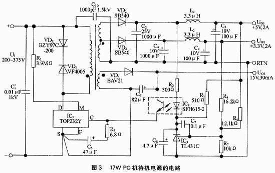
The PC standby power supply circuit that can provide two main outputs of 5V, 2A and 3.3V, 2A is shown in Figure 3. The power supply also adds an auxiliary output of 15V, 30mA at the lowest cost. A TOP232Y single-chip switching power supply is used in the circuit, and the total output power is 17.05W. The DC input voltage range is 200-375V. A 220/110V AC fixed input voltage can also be selected, and only a rectifier filter is connected, without adding an input voltage doubler to double the 110V AC. This design gives full play to the excellent characteristics of TOP232Y such as soft start, undervoltage protection, strict current limiting characteristics and high switching frequency, so that the high-frequency transformer can select EE19 type magnetic core. In addition, since TOP232Y increases the distance between the high-voltage drain terminal and the low-voltage terminal, the leakage between the pins is reduced, so the power supply can be used in a harsh environment. C1 is a high-frequency decoupling capacitor for DC high voltage, and C1 can be omitted when U1 is very close to the standby power supply. The line detection circuit R1 is used to set the undervoltage value UUV. When R1=3.9MΩ , UUV=IUV·R1=50 μA×3.9MΩ=UI>195V DC , the power supply is reconnected.
The feedback winding voltage is rectified and filtered by VD4 and C6 to generate a 15V feedback voltage, which is used as a +15V output (not isolated from the primary) on the one hand, and provides bias to the control end of TOP232Y through a phototransistor on the other hand. R4, R6 and R7 are sampling resistors used to detect the change in the output voltage of 3.3V and 5V. R2 is the limiter of the LED TL431C provides bias current. C8 is a soft-start capacitor that can eliminate the voltage overshoot phenomenon generated when the power is just turned on. The feature of TOP232Y skipping cycles when unloaded can meet the low power consumption index of the PC standby power supply.
Previous article:Design and implementation of a digitally controlled DC current source
Next article:Electromagnetic compatibility design based on TOPSwitCh
- MathWorks and NXP Collaborate to Launch Model-Based Design Toolbox for Battery Management Systems
- STMicroelectronics' advanced galvanically isolated gate driver STGAP3S provides flexible protection for IGBTs and SiC MOSFETs
- New diaphragm-free solid-state lithium battery technology is launched: the distance between the positive and negative electrodes is less than 0.000001 meters
- [“Source” Observe the Autumn Series] Application and testing of the next generation of semiconductor gallium oxide device photodetectors
- 采用自主设计封装,绝缘电阻显著提高!ROHM开发出更高电压xEV系统的SiC肖特基势垒二极管
- Will GaN replace SiC? PI's disruptive 1700V InnoMux2 is here to demonstrate
- From Isolation to the Third and a Half Generation: Understanding Naxinwei's Gate Driver IC in One Article
- The appeal of 48 V technology: importance, benefits and key factors in system-level applications
- Important breakthrough in recycling of used lithium-ion batteries
- Innolux's intelligent steer-by-wire solution makes cars smarter and safer
- 8051 MCU - Parity Check
- How to efficiently balance the sensitivity of tactile sensing interfaces
- What should I do if the servo motor shakes? What causes the servo motor to shake quickly?
- 【Brushless Motor】Analysis of three-phase BLDC motor and sharing of two popular development boards
- Midea Industrial Technology's subsidiaries Clou Electronics and Hekang New Energy jointly appeared at the Munich Battery Energy Storage Exhibition and Solar Energy Exhibition
- Guoxin Sichen | Application of ferroelectric memory PB85RS2MC in power battery management, with a capacity of 2M
- Analysis of common faults of frequency converter
- In a head-on competition with Qualcomm, what kind of cockpit products has Intel come up with?
- Dalian Rongke's all-vanadium liquid flow battery energy storage equipment industrialization project has entered the sprint stage before production
- Allegro MicroSystems Introduces Advanced Magnetic and Inductive Position Sensing Solutions at Electronica 2024
- Car key in the left hand, liveness detection radar in the right hand, UWB is imperative for cars!
- After a decade of rapid development, domestic CIS has entered the market
- Aegis Dagger Battery + Thor EM-i Super Hybrid, Geely New Energy has thrown out two "king bombs"
- A brief discussion on functional safety - fault, error, and failure
- In the smart car 2.0 cycle, these core industry chains are facing major opportunities!
- The United States and Japan are developing new batteries. CATL faces challenges? How should China's new energy battery industry respond?
- Murata launches high-precision 6-axis inertial sensor for automobiles
- Ford patents pre-charge alarm to help save costs and respond to emergencies
- New real-time microcontroller system from Texas Instruments enables smarter processing in automotive and industrial applications
- Understanding damper actuators and what drives them in automotive HVAC systems
- [TI recommended course] #Live replay: Application of TI millimeter wave sensors in smart home#
- Anti-reverse connection design for low power consumption Anti-reverse connection and anti-backflow circuit design,,,,
- [GD32450I-EVAL] Unpack and power on to build a development environment
- 【Drawing board experience】 PCB design skills of switching power supply
- The history and concept of radio and its key technologies
- Help
- Failed experience of using BlueNRG-1 to make a BLE chicken-eating tool
- Exploiting software vulnerabilities! 19-year-old boy remotely hacked into Tesla
- Gizwits GoKit 3 Hardware Manual

 AUTOSAR MCAL Principles and Practice
 Cortex Microcontroller Software Interface Standard (CMSIS)


 京公网安备 11010802033920号