From a power budget perspective, the radio frequency power amplifier (RF PA) powered directly by the battery is an important component to consider. Traditionally, RF power amplifiers used in CDMA/WCDMA cellular standards have been directly powered by batteries. This power supply method makes the system easy to design. However, the actual efficiency of the linear power amplifiers used in this standard over the entire transmit power range Very low. This article describes a solution to provide efficient RF PA system power management through DC/DC converters.
With the continuous development of cellular standards, the transmission rate has developed from 14.4kbps in the CDMA-1 standard to 2Mbps in the CDMA2000/WCDMA standard. In addition, in order to increase the average revenue obtained from each user, cellular communication operators have begun to increase 3G phone-related services. At the same time, talk time and battery life are also expected to be improved by using batteries with the same or slightly higher capacity. This makes system design more challenging. System designers must be very careful to examine the power of every component on the mobile phone circuit board. From a power budget perspective, the radio frequency power amplifier (RF PA) powered directly by the battery is an important component to consider.
The modulation circuitry used in CDMA and WCDMA results in the generation of an AM signal that exhibits a non-constant amplitude envelope. To maintain signal integrity and facilitate spectrum regeneration, a linear power amplifier is required. However, since the power amplifier can only maintain high efficiency when operating under gain compression conditions, the conversion efficiency is not high. To achieve the required linearity, the actual transmit power is compensated from the power amplifier's compression point, which results in an overall reduction in efficiency. When the mobile phone works in transmitting mode, due to the low actual efficiency of the power amplifier, the power consumption of the radio frequency part will account for 65% of the total power budget.
 |
|
Figure 1: Old vs. new methods |
Therefore, using a magnetic buck converter for power supply is an ideal choice for linear power amplifiers, which will greatly improve the efficiency of the system. Increased power efficiency (PAE) is the primary performance indicator of power amplifiers.
PAE(%)= (POUT-PIN)/Pdc
The main purpose of using a DC-DC converter (power amplifier power regulator) is to reduce the Pdc factor in the denominator. When the power amplifier is directly connected to the battery, Pdc=Vbatt*Ibatt, and when it is powered by the power amplifier power regulator, Pdc=V o *I o . Now we can see that in order to increase PAE, Vo and I must be lower than Vbatt and Ibatt. This can be accomplished by reducing the transmitted RF power level and reducing the output voltage of the power amplifier supply regulator. This also reduces I o (the current absorbed by the power amplifier), and due to the high efficiency of the DC-DC converter, the output current of the battery is also reduced.
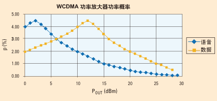
To truly understand the power savings a power regulator brings to a power amplifier, it is important to consider power probability plots for different modulation methods (see Figure 2). Power probability maps will differ in urban and rural areas.
 |
|
Figure 2: In a standard mobile phone, the power amplifier emits at low power levels most of the time. Using a power amplifier supply voltage regulator increases the probability of power savings. |
As shown in Figure 3, in order to meet the adjacent channel power rejection ratio (ACPR) requirements, the output voltage of the DC-DC converter must change as the transmit power level changes. Battery current can be saved up to 50mA over the power level range of 0d Bm to 20d Bm. Figure 2 shows that the power amplifier operates within this power level range most of the time.
 |
|
Figure 3: Battery current savings when the power amplifier is powered by a DC-DC converter |
 |
|
Figure 4: Percent power savings when the power amplifier is powered by a power regulator |
So why do we have to change the voltage of the DC-DC converter when the transmit power level increases? The answer is: This change is needed to maintain the Adjacent Channel Power Rejection Ratio (ACPR). ACPR is used to indicate the distortion condition of the power amplifier and the tendency of other subsystems or systems to cause adjacent channel interference. It refers to the ratio of the power spectral density (PSD) of the main channel to the power spectral density measured at several different offset frequencies.
 |
|
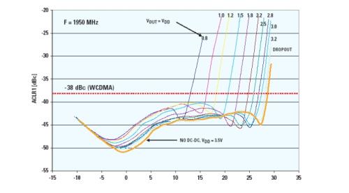
Figure 5: How the power amplifier’s supply voltage and POUT affect ACLR |
Figure 5 shows that when P out increases, if the supply voltage of the power amplifier does not increase, the performance index of ACLR cannot meet the requirements.
The system-level indicator (3 GPP) of WCDMA is -34d Bc. In order to maintain sufficient margin (caused by differences in temperature and devices), the value of ACLR is generally set at -38d Bc.
Key Requirements for Buck Converters Powering RF Power Amplifiers
The buck converter that powers the RF power amplifier has special functions that are very different from the buck converter that powers the digital core processor. They differ mainly in operating characteristics and parameters such as switching FET on-resistance, current limit, transient response, operating mode (such as PFM/PWM), start-up time, quiescent current and voltage drop. The following examples illustrate these differences:
High efficiency over a wide range of output voltage and load range
Example: When VIN=4.2V, V o =3.4V, I o =400mA (high RF power), the efficiency of LM3205 reaches 96%, when VIN=3.9V, V o =1.5V, I o =100mA (low RF power), the efficiency is 87%.
Example: The V con pin can be used to adjust the output voltage of LM3205 between 0.8V and 3.6V. The voltage gain from V con to Vo is 2.5.
Example: A low R DSON (140 mΩ) PFET (LM3205) or bypass FET (LM3024) produces low voltage drop, pulse omitting circuitry for low ripple at near 100% duty cycle.
Example: A minimum on-time of 50 nanoseconds enables 10% duty cycle operation and an output voltage of 0.8V or less. Of course, this depends on the range of V IN .
Example: A 2MHz switching frequency enables the use of smaller external components and meets spectrum emission requirements.
Example: When V 0 =3.4V, when EN changes from low to high, the on-time of LM3203 is 50 microseconds.
100% duty cycle vs. bypass mode
When the buck converter is operating at 100% duty cycle, the voltage drop is:
Voltage drop = (RON,P+RL)·IO,
Here, R ON,P is the RDSON of the PFET and R L is the DCR of the inductor. For a power amplifier power regulator with a bypass FET, the voltage drop in bypass mode is:
Voltage drop = (RON, BYP)·IO,
Here, R ON,BYPDSON DSON
application circuit example
As shown in Figure 6, in this example, the baseband has a lookup table circuit that sets the output voltage based on the desired output power level.
 |
|
Figure 6: Baseband directly controls Vo |
In the case of Figure 7, the power detector is part of the closed loop and sets the output voltage.
 |
|
Figure 7: Using the power detector to set Vo |
in conclusion
DC-DC converters improve the efficiency of RF power amplifier systems in handheld mobile devices and enable additional features and functionality through increased battery life.
Previous article:Boost digitally controlled power supply performance with smart MOSFET drivers
Next article:Overcurrent protection of power modules
Recommended ReadingLatest update time:2024-11-16 16:52


- Popular Resources
- Popular amplifiers
-
 Multimodal perception parameterized decision making for autonomous driving
 -
 Semantic Segmentation for Autonomous Driving: Model Evaluation, Dataset Generation, Viewpoint Comparison, and Real-time Performance
 -
 Monocular semantic map localization for autonomous vehicles
 -
 Hardware Accelerators in Autonomous Driving
- MathWorks and NXP Collaborate to Launch Model-Based Design Toolbox for Battery Management Systems
- STMicroelectronics' advanced galvanically isolated gate driver STGAP3S provides flexible protection for IGBTs and SiC MOSFETs
- New diaphragm-free solid-state lithium battery technology is launched: the distance between the positive and negative electrodes is less than 0.000001 meters
- [“Source” Observe the Autumn Series] Application and testing of the next generation of semiconductor gallium oxide device photodetectors
- 采用自主设计封装,绝缘电阻显著提高!ROHM开发出更高电压xEV系统的SiC肖特基势垒二极管
- Will GaN replace SiC? PI's disruptive 1700V InnoMux2 is here to demonstrate
- From Isolation to the Third and a Half Generation: Understanding Naxinwei's Gate Driver IC in One Article
- The appeal of 48 V technology: importance, benefits and key factors in system-level applications
- Important breakthrough in recycling of used lithium-ion batteries
- Innolux's intelligent steer-by-wire solution makes cars smarter and safer
- 8051 MCU - Parity Check
- How to efficiently balance the sensitivity of tactile sensing interfaces
- What should I do if the servo motor shakes? What causes the servo motor to shake quickly?
- 【Brushless Motor】Analysis of three-phase BLDC motor and sharing of two popular development boards
- Midea Industrial Technology's subsidiaries Clou Electronics and Hekang New Energy jointly appeared at the Munich Battery Energy Storage Exhibition and Solar Energy Exhibition
- Guoxin Sichen | Application of ferroelectric memory PB85RS2MC in power battery management, with a capacity of 2M
- Analysis of common faults of frequency converter
- In a head-on competition with Qualcomm, what kind of cockpit products has Intel come up with?
- Dalian Rongke's all-vanadium liquid flow battery energy storage equipment industrialization project has entered the sprint stage before production
- Allegro MicroSystems Introduces Advanced Magnetic and Inductive Position Sensing Solutions at Electronica 2024
- Car key in the left hand, liveness detection radar in the right hand, UWB is imperative for cars!
- After a decade of rapid development, domestic CIS has entered the market
- Aegis Dagger Battery + Thor EM-i Super Hybrid, Geely New Energy has thrown out two "king bombs"
- A brief discussion on functional safety - fault, error, and failure
- In the smart car 2.0 cycle, these core industry chains are facing major opportunities!
- The United States and Japan are developing new batteries. CATL faces challenges? How should China's new energy battery industry respond?
- Murata launches high-precision 6-axis inertial sensor for automobiles
- Ford patents pre-charge alarm to help save costs and respond to emergencies
- New real-time microcontroller system from Texas Instruments enables smarter processing in automotive and industrial applications
- Newbie help, the light flashes five times, the buzzer sounds once, now it flashes and sounds
- An 80W power amplifier for LS band, equalizer adjustment
- Protel99 generates a network table where some components have no connections
- Common problems in debugging the TMS320C3x series?
- Regarding GaN devices, these issues should be paid attention to!
- 【GD32E231_DIY】-02: Development environment construction and creating a new project
- TI C64X DSP interrupt vector table configuration (hardware interrupt)
- Taking a “family-first” approach to op amp design
- Who knows the name of the chip?
- Pre-match training FAQ: Detailed explanation of ON Semiconductor's ultra-low power RSL10 Bluetooth SoC development board

 Multimodal perception parameterized decision making for autonomous driving


 京公网安备 11010802033920号