With the advancement of the dual carbon goals, electric vehicle on-board chargers (hereinafter referred to as "OBCs") are developing in the direction of bidirectional energy transmission, which can both obtain power from the grid and feed power back to the grid. Electric vehicles equipped with bidirectional OBCs can use the remaining power to charge depleted electric vehicles, can also serve as a 220 V power supply outdoors, and can also be used as distributed energy storage stations to help the grid eliminate peak loads and fill valleys. This article will explore the design challenges of the CLLC topology in bidirectional OBC applications and how the 6.6 kW CLLC reference design from Onsemi solves these challenges.
What is CLLC topology
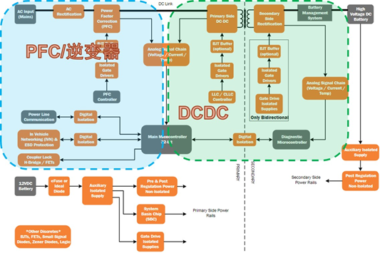
As shown in Figure 1, isolated DCDC is one of the main components of bidirectional OBC. In isolated DCDC applications above 200 W, including unidirectional OBC, many use LLC topology because of its advantages such as high energy efficiency, good EMI performance, and low development difficulty, but this topology can only be used for unidirectional energy transmission.

Figure 1: Bidirectional OBC block diagram
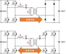
Most bidirectional OBCs use the CLLC topology for the isolated DCDC stage. The CLLC topology (as shown in Figure 2) replaces the bridge rectifier diode on the battery side of the LLC topology with an active bridge, and then connects a C in series on the battery end of the transformer to ensure magnetic balance. When charging the battery, the bridge on the left is an active switch and the bridge on the right is a synchronous rectifier; when the battery is inverted, the bridge on the right is an active switch and the bridge on the left is a synchronous rectifier. CLLC inherits the characteristics of the LLC topology, uses pulse frequency regulation to control the gain, and has the same soft switching characteristics. Therefore, it has high energy efficiency, good EMI performance, and is simple, but there are challenges such as a narrow gain adjustment range and difficulty in meeting a wide battery voltage variation range. To this end, ON Semiconductor has launched a 6.6 kW CLLC reference design SEC-6K6W-CLLC-GEVK, which uses a wide bus voltage range to cope with battery voltage changes, with a peak energy efficiency of more than 98%, helping designers solve challenges and accelerate development.

Figure 2: CLLC topology

Figure 3: The 6.6 kW CLLC reference design SEC-6K6W-CLLC-GEVK has a peak efficiency of over 98%
6.6 kW CLLC reference design SEC-6K6W-CLLC-GEVK
ON Semiconductor's 6.6 kW CLLC reference design SEC-6K6W-CLLC-GEVK consists of three main parts, as shown in Figure 4: The large board in the middle is the power board, and all high-voltage and high-current lines are on this board. The upper right corner is the control board, which is connected to the power board through connectors, making it convenient for everyone to cross-test between different control and power solutions. On the left is the resonant cavity combination, which includes a transformer with an integrated resonant inductor and two resonant capacitor plates. The resonant capacitor is composed of multiple MLCCs connected in series and parallel to achieve a smaller size while meeting the requirements of withstand voltage and current. The resonant cavity is also detachable, which is convenient for designers to verify different transformer, inductor and capacitor parameters. The solution includes a heat sink, fan, auxiliary power supply, protection circuit, etc. Connecting the power supply and load allows long-term testing at full load.

Figure 4: 6.6 kW CLLC reference design SEC-6K6W-CLLC-GEVK
In the power board, the two active bridges located on the bus side and the battery side are composed of four 1200 V/40 milliohm NVHL040N120SC1 and four 900 V/20 milliohm NVHL020N090SC1 silicon carbide (SiC) MOS. SiC can achieve higher power density, higher switching frequency and extremely efficient design than Si. The eight SiC MOS are driven by eight magnetically isolated high current drivers . The drive signal is sent by the control board through the control interface.
All signals of the control interface are located on the battery side, and the voltage level does not exceed 12 V. The voltage and current of the battery end are directly sent to the control interface after sampling, voltage division and amplification. The voltage sampling on the bus side is completed by an independent ADC, and the data is transmitted to the control interface through the SPI bus and the digital signal isolator.
In the control board, we selected an automotive-grade LLC control chip NCV4390 to perform pulse frequency modulation (hereinafter referred to as "PFM") and synchronous rectification control; a low-power MCU to set the constant voltage value for charging; an automotive-grade rail-to-rail op amp NCV33204 to perform constant current charging control; and our automotive-grade logic devices to judge and convert the direction from grid to battery and from battery to grid.
Design considerations for circuit details
If you want to save costs, you can replace 1200 V and 900 V SiC MOS with 900 V and 650 V SiC MOS, but you need to control the switching spikes. It is best to start by reducing the PCB parasitic inductance, which can be achieved by adding bypass capacitors.
The high-voltage, low-Rdson SiC MOSFET has a large Qg. In order to maintain high efficiency at high switching frequencies, it must be driven by a high-current gate driver. In addition, the control interface of our solution is located on the battery side, and the MOS on the driving bus side must be isolated and comply with safety regulations. Although the MOS on the driving battery side does not require safety regulations, in order to unify materials, we still choose the same device NCV57000, whose short-circuit protection and fault reporting functions are its highlights.
Another good choice for isolated gate driver is NCV51561, which also has safety isolation, higher drive current, one-to-two, and shorter delay. Although it does not have overcurrent protection, its double high prohibition function can also protect the risk of explosion caused by interference or misoperation from the signal end.
Selecting the best topology for high voltage auxiliary power supply
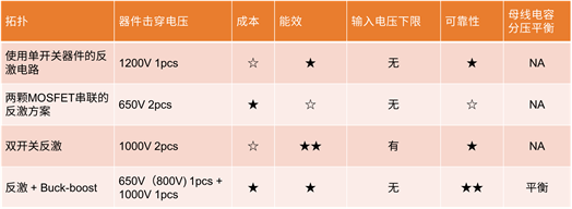
The auxiliary power supply of this 6.6 kW CLLC reference design adopts the "flyback + Buck-boost" topology to cope with the bus voltage up to 750 V. As shown in Table 1, compared with the other three topologies, this flyback + Buck-boost topology is superior in cost, energy efficiency, input voltage lower limit, reliability, and bus capacitor voltage balance.

Table 1: Available high voltage auxiliary power supply topologies at 800 V input voltage
Choosing the best solution for powering high-side gate drivers
Another challenge in auxiliary power design is multiple and isolated power rails. The 6.6 kW CLLC reference design requires a total of 7 power rails.
SiC drive requires negative voltage, and the Vcc tolerance range of SiC MOS is narrow, so bootstrapping is not suitable, otherwise it will bring many problems such as voltage regulation, timing, power consumption, noise, etc. If isolated DCDC is used, there will be problems such as PCB space occupation, cost and noise interference. The third method is to output all voltages through the transformer winding. This is the lowest cost of these methods, but the disadvantage is that the process is not well controlled, prone to errors, and has large noise interference. The pulse transformer extended winding used in our 6.6 kW CLLC reference design solves all the problems of the above three methods, and more importantly, it greatly shortens the length of the moving point lead.
Dual-edge tracking adaptive synchronous rectification control
As mentioned above, the LLC controller NCV4390 is used in the control board to control the PFM loop and synchronous rectification. NCV4390 uses current mode, has fast loop response, is not easy to oscillate, and has a built-in dual-edge tracking synchronous rectification control function. A PWM working mode is inserted between the PFM mode and the intermittent working mode to improve the energy efficiency and voltage ripple under light load. In addition, the protection function of NCV4390 is also very powerful. It is worth emphasizing that this dual-edge tracking synchronous rectification control method has been verified by the market and is very reliable.
Summarize
Electric vehicle OBC is developing towards bidirectional energy transmission to match the advancement of dual carbon goals. Isolated DCDC is one of the main components of bidirectional OBC. Most of the isolated DCDC levels in bidirectional OBCs will adopt the CLLC topology. ON Semiconductor's 6.6 kW CLLC reference design SEC-6K6W-CLLC-GEVK, based on SiC MOS, has a peak energy efficiency of over 98%. It also solves many design challenges of CLLC topology in bidirectional OBC applications, such as PCB footprint, noise interference, reliability and cost. It uses a hardware controller for PFM control to help designers speed up development. More information, including bill of materials (BOM), circuit diagrams, Gerber files and test reports
Previous article:CS5918 Switching Type 2A Single Cell 4.2V Li-ion Battery Charge Management IC Solution
Next article:Wireless charging technology for mobile robots enables Industry 4.0
Recommended ReadingLatest update time:2024-11-16 12:46


- Popular Resources
- Popular amplifiers
-
 Optimized drivetrain and new semiconductor technologies enable the design of energy-efficient electr
 -
 Chip Manufacturing: A Practical Tutorial on Semiconductor Process Technology (Sixth Edition)
 -
 TOWARDS CMOS NUCLEAR MAGNETIC RESONANCE SPECTROSCOPY DESIGN, IMPLEMENTATION AND EXPERIMENTAL RESULTS
 -
 RSL10 Environmental Expert Smart Watch
- MathWorks and NXP Collaborate to Launch Model-Based Design Toolbox for Battery Management Systems
- STMicroelectronics' advanced galvanically isolated gate driver STGAP3S provides flexible protection for IGBTs and SiC MOSFETs
- New diaphragm-free solid-state lithium battery technology is launched: the distance between the positive and negative electrodes is less than 0.000001 meters
- [“Source” Observe the Autumn Series] Application and testing of the next generation of semiconductor gallium oxide device photodetectors
- 采用自主设计封装,绝缘电阻显著提高!ROHM开发出更高电压xEV系统的SiC肖特基势垒二极管
- Will GaN replace SiC? PI's disruptive 1700V InnoMux2 is here to demonstrate
- From Isolation to the Third and a Half Generation: Understanding Naxinwei's Gate Driver IC in One Article
- The appeal of 48 V technology: importance, benefits and key factors in system-level applications
- Important breakthrough in recycling of used lithium-ion batteries
- Innolux's intelligent steer-by-wire solution makes cars smarter and safer
- 8051 MCU - Parity Check
- How to efficiently balance the sensitivity of tactile sensing interfaces
- What should I do if the servo motor shakes? What causes the servo motor to shake quickly?
- 【Brushless Motor】Analysis of three-phase BLDC motor and sharing of two popular development boards
- Midea Industrial Technology's subsidiaries Clou Electronics and Hekang New Energy jointly appeared at the Munich Battery Energy Storage Exhibition and Solar Energy Exhibition
- Guoxin Sichen | Application of ferroelectric memory PB85RS2MC in power battery management, with a capacity of 2M
- Analysis of common faults of frequency converter
- In a head-on competition with Qualcomm, what kind of cockpit products has Intel come up with?
- Dalian Rongke's all-vanadium liquid flow battery energy storage equipment industrialization project has entered the sprint stage before production
- Allegro MicroSystems Introduces Advanced Magnetic and Inductive Position Sensing Solutions at Electronica 2024
- Car key in the left hand, liveness detection radar in the right hand, UWB is imperative for cars!
- After a decade of rapid development, domestic CIS has entered the market
- Aegis Dagger Battery + Thor EM-i Super Hybrid, Geely New Energy has thrown out two "king bombs"
- A brief discussion on functional safety - fault, error, and failure
- In the smart car 2.0 cycle, these core industry chains are facing major opportunities!
- The United States and Japan are developing new batteries. CATL faces challenges? How should China's new energy battery industry respond?
- Murata launches high-precision 6-axis inertial sensor for automobiles
- Ford patents pre-charge alarm to help save costs and respond to emergencies
- New real-time microcontroller system from Texas Instruments enables smarter processing in automotive and industrial applications
- bluenrg-2 cannot connect to other devices directly when it is the host
- Playing with Zynq Serial 43——[ex62] Image Laplace Edge Extraction of OV5640 Camera
- [NXP Rapid IoT Review] + First try of mobile APP
- CC2541 Key Fob Reference Design
- Give feedback on Lingdong Micro's MM32F013x library functions and routines
- Design of wireless voice communication system based on Mesh technology
- [Domestic RISC-V Linux Board Fang·Starlight VisionFive Trial Report] Environment Preparation——Install MySQL
- Project Management (Passive Components)
- Could you please tell me what is the name of the plastic film wrapped around the outside of the transformer?
- About the power supply of the circuit board

 Optimized drivetrain and new semiconductor technologies enable the design of energy-efficient electr
 RSL10 Environmental Expert Smart Watch


 京公网安备 11010802033920号