By Edward Ong, Senior Product Marketing Manager, Power Integrations
Power supply designers today face two main issues: eliminating harmful input harmonic currents and ensuring that the power factor is as close to unity as possible. Harmful harmonic currents can cause overheating of transmission equipment and create interference problems that must subsequently be resolved; both of which can also adversely affect the size and/or efficiency of the circuit. If the load applied to the line is not purely resistive, a phase shift will occur between the input voltage and current waveforms, increasing the apparent power and reducing transmission efficiency. If nonlinear loads distort the input current waveform, current harmonics will be introduced, further reducing transmission efficiency and introducing interference into the utility grid.
To solve these problems, you need to understand the basic principles of power conversion. In a power supply, the AC voltage from the wall socket is usually connected to a rectifier circuit, which converts the AC voltage into an AC signal with a fixed polarity and a peak voltage equivalent to a fixed VDC voltage. The signal is fed into a large capacitor to form a filter that smoothes the ripples in the voltage waveform. The newly generated DC signal is fed to the DC/DC converter stage of the power supply to achieve the low-voltage DC required for the final output.
If we go back to the original rectifier stage and look at the waveform, the input AC voltage is a traditional symmetrical sine wave with alternating positive and negative poles. However, the input current appears as a series of spikes that increase as the input voltage rises. This is because the diode conduction (and therefore current flow) only occurs when the large capacitor is charged, when the VAC input voltage exceeds the DC voltage stored on the capacitor. When VAC is lower than the stored capacitor voltage, the charge stored on the large capacitor will support the output of the power supply. During this time, energy is transferred from the capacitor to the load, which causes the capacitor voltage to drop. Once the AC voltage exceeds the (now lower) voltage on the energy storage capacitor again, the capacitor will recharge. This short charging window means that the input current is provided in the form of triangular pulses rather than a sine wave.

Figure 1: The input current to the rectifier stage appears as a series of spikes with a lot of harmonic content, which pollutes the AC line.
This peak current waveform consists of a series of power frequency harmonics. Harmonic content is limited by various national and international regulations established to protect distribution networks. The power factor of the circuit shown in Figure 1 is often very low, about 0.5, far from the ideal 1.
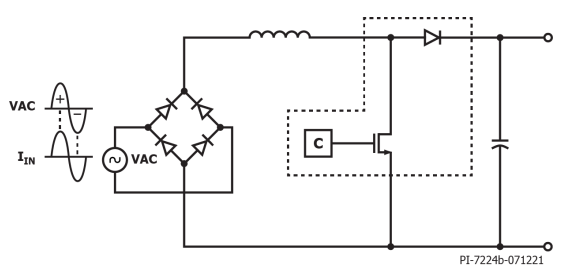
This problem can be solved in a few different ways. The simplest way is to add an inductor to cancel out the capacitive component of the circuit - a technique known as passive power factor correction. However, passive power correction can only do so much. In applications with high power output, the physical size of the required inductor makes it impractical. In such cases, an active PFC circuit is often used to bring the circuit's power factor closer to unity without negatively affecting the size of the circuit. Active power factor correction consists of a PFC diode, an inductor, and a MOSFET. The MOSFET acts as a high-frequency switch, driven by a controller that executes the power factor correction algorithm.
The switching circuit forces the input current to follow the rectified VAC input and become a proper sine wave again. Ideally, the sine wave has low distortion to eliminate harmonic currents that can pollute the AC line. Since the voltage and current waveforms are in phase, the power factor also rises to nearly the ideal value of 1.

Figure 2: A rectifier stage with active power factor correction converts the input current into a sine wave
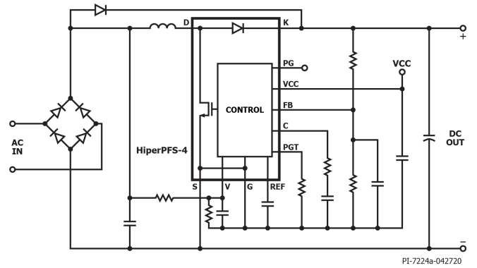
A simple way to implement an active PFC circuit is to use the HiperPFS-4 solution from Power Integrations (see Figure 3). The HiperPFS-4 device includes an ultra-low reverse recovery charge diode to achieve high efficiency by minimizing the diode's conversion losses. It also features a low RDS(ON) MOSFET that reduces conduction losses and an advanced continuous conduction mode controller that integrates many safety features.

Figure 3: Power Integrations’ HiperPFS-4
HiperPFS-4 devices integrate power factor correction diodes, MOSFETs and controllers at the same time. This high level of integration helps reduce development time and speed up time to market. Another advantage of integrating key components in one package is to minimize parasitic inductance in the wiring. The reduction in circuit inductance helps reduce the voltage stress across the PFC diode and the peak drain-source voltage of the MOSFET, thereby improving the reliability of the circuit. In addition, the diodes used have soft recovery characteristics that reduce ringing, thereby reducing EMI. Integrating the diode and MOSFET in one package can significantly reduce the loop size, further reducing EMI.

Figure 4: The HiperPFS-4 device integrates key components for active power factor correction in the same package.
To minimize parasitic inductance in the wiring, thereby reducing di/dt induced voltage stress on the power switch
Summarize
Active power factor correction is the best way to reduce harmful input harmonic currents and improve power factor. Power Integrations has developed the HiperPFS-4 solution, which integrates the key components required for active power factor correction into the same package. This solution can significantly reduce input current harmonics and improve power factor, while solving many layout issues common in traditional circuit designs, such as reducing voltage stress, EMI and parasitic losses.
Previous article:eGaN® FET-based 50 W, 12 V/60 V Boost Converter
Next article:TI's new supercapacitor charging and discharging integrated buck/boost converter
- MathWorks and NXP Collaborate to Launch Model-Based Design Toolbox for Battery Management Systems
- STMicroelectronics' advanced galvanically isolated gate driver STGAP3S provides flexible protection for IGBTs and SiC MOSFETs
- New diaphragm-free solid-state lithium battery technology is launched: the distance between the positive and negative electrodes is less than 0.000001 meters
- [“Source” Observe the Autumn Series] Application and testing of the next generation of semiconductor gallium oxide device photodetectors
- 采用自主设计封装,绝缘电阻显著提高!ROHM开发出更高电压xEV系统的SiC肖特基势垒二极管
- Will GaN replace SiC? PI's disruptive 1700V InnoMux2 is here to demonstrate
- From Isolation to the Third and a Half Generation: Understanding Naxinwei's Gate Driver IC in One Article
- The appeal of 48 V technology: importance, benefits and key factors in system-level applications
- Important breakthrough in recycling of used lithium-ion batteries
- Innolux's intelligent steer-by-wire solution makes cars smarter and safer
- 8051 MCU - Parity Check
- How to efficiently balance the sensitivity of tactile sensing interfaces
- What should I do if the servo motor shakes? What causes the servo motor to shake quickly?
- 【Brushless Motor】Analysis of three-phase BLDC motor and sharing of two popular development boards
- Midea Industrial Technology's subsidiaries Clou Electronics and Hekang New Energy jointly appeared at the Munich Battery Energy Storage Exhibition and Solar Energy Exhibition
- Guoxin Sichen | Application of ferroelectric memory PB85RS2MC in power battery management, with a capacity of 2M
- Analysis of common faults of frequency converter
- In a head-on competition with Qualcomm, what kind of cockpit products has Intel come up with?
- Dalian Rongke's all-vanadium liquid flow battery energy storage equipment industrialization project has entered the sprint stage before production
- Allegro MicroSystems Introduces Advanced Magnetic and Inductive Position Sensing Solutions at Electronica 2024
- Car key in the left hand, liveness detection radar in the right hand, UWB is imperative for cars!
- After a decade of rapid development, domestic CIS has entered the market
- Aegis Dagger Battery + Thor EM-i Super Hybrid, Geely New Energy has thrown out two "king bombs"
- A brief discussion on functional safety - fault, error, and failure
- In the smart car 2.0 cycle, these core industry chains are facing major opportunities!
- The United States and Japan are developing new batteries. CATL faces challenges? How should China's new energy battery industry respond?
- Murata launches high-precision 6-axis inertial sensor for automobiles
- Ford patents pre-charge alarm to help save costs and respond to emergencies
- New real-time microcontroller system from Texas Instruments enables smarter processing in automotive and industrial applications
- Is the intelligent express delivery pickup system based on LabVIEW not too complicated?
- How to implement ship mode in Li-ion battery designs
- Read the good book "The Self-Taught Handbook for Electronic Engineers" - Mastery Edition
- What is the function of the DET signal?
- Several issues with the tps65130 chip
- B-U585I-IOT02A Bluetooth problem solved
- Share the November 2018 STMicroelectronics-Shunde Motor Control Roadshow Conference Brochure
- My Journey of MCU Development (V)
- Why should we apply synchronous rectification technology?
- Can you return home during the 2022 Spring Festival? It is difficult for people in these provinces to return home, so people returning home should pay attention

 Three-Phase 11 kW PFC + LLC Electric Vehicle On-Board Charging (OBC) Platform User Manual (ONSEMI Semiconductor)
 開關電源專業英語
 Classic EMI Filter Design Second Edition


 京公网安备 11010802033920号