1. Introduction
With the increasing popularity of automobiles, some electrical appliances with 220V/50Hz AC as input cannot be directly used in cars powered by 12VDC batteries, which greatly limits the scope of use of these appliances and brings many inconveniences to people's lives. Therefore, it has become a demand to develop an economical and practical vehicle-mounted inverter. As a power supply device for various electronic products, the quality of the vehicle-mounted power supply greatly affects the reliability of electronic equipment. The conversion efficiency and load capacity are directly related to its application scope. At present, vehicle-mounted inverters usually use DC/DC high-frequency boost part and DC/AC inverter two-stage control, among which DC/AC inverter has two types: SPWM inverter and square wave inverter. The former has low output voltage and low harmonic content, small output filter size, but complex control and low overall efficiency; the latter has low output voltage and high harmonic content, large output filter size, simple and reliable control and high efficiency.
This article introduces the design of a car inverter based on the control chip LM25037. Its main parameters are as follows:
Input voltage: 9.6~16.2VDC
Output voltage: 220V (±5V) 50Hz (±0.5%) AC
Output power: 150W
2. Basic structure of the circuit
The input end of this inverter power supply is a battery (+12V, capacity 90A·h), and the output end is an industrial frequency square wave voltage (50Hz, 220V). Its structural block diagram is shown in Figure 1. At present, there are many new technologies that constitute DC/AC inversion, but considering the complexity, cost and reliability of control, this power supply still uses a typical two-stage conversion, namely DC/DC conversion and DC/AC inversion. First, the DC12V voltage is inverted into a high-frequency square wave by DC/DC conversion, which is boosted by a high-frequency transformer and then rectified and filtered to obtain a stable DC voltage of about 310V; then the DC/AC conversion uses a square wave inversion method to invert the stable DC voltage into a square wave voltage with an effective value slightly greater than 220V; and then the LC industrial frequency filter obtains a 50Hz AC voltage with an effective value of 220V to drive the load.
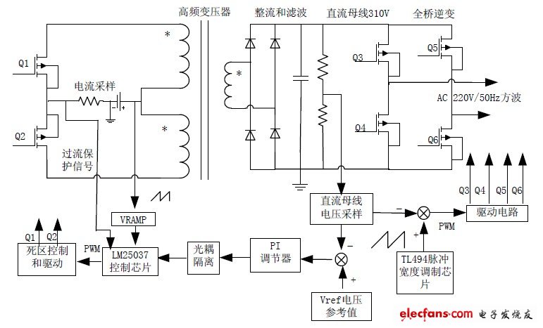
Figure 1 System structure diagram
3. Circuit design
3.1 DC/DC Converter Design
Since the primary voltage of the transformer is low, a push-pull circuit is used to improve the utilization rate of the transformer. The center tap is connected to the battery, and the two ends are connected to Q1 and Q2 switch tubes to work alternately to improve the conversion efficiency of the system. The push-pull circuit uses fewer switching devices, reduces the size of the transformer, and increases the output power.
3.1.1 Introduction to control chip
The DC/DC converter uses the 16-pin control chip LM25037 developed by National Semiconductor Corporation (NSC) for portable power systems in vehicles. The chip has the following features: voltage mode control; internal integration of a 75V startup bias regulator; generation of a feedforward PWM sawtooth wave; programmable undervoltage protection with hysteresis characteristics; overcurrent protection with a timer dual mode with a delay and timed restart after protection, and the restart time is set by the user; programmable maximum duty cycle and soft start; internal integration of a high-precision error amplifier and overcurrent comparator, with external synchronization and other functions; two-way alternating output drive signals, suitable for push-pull, full-bridge and half-bridge topologies. The internal structure of the chip is shown in Figure 2.
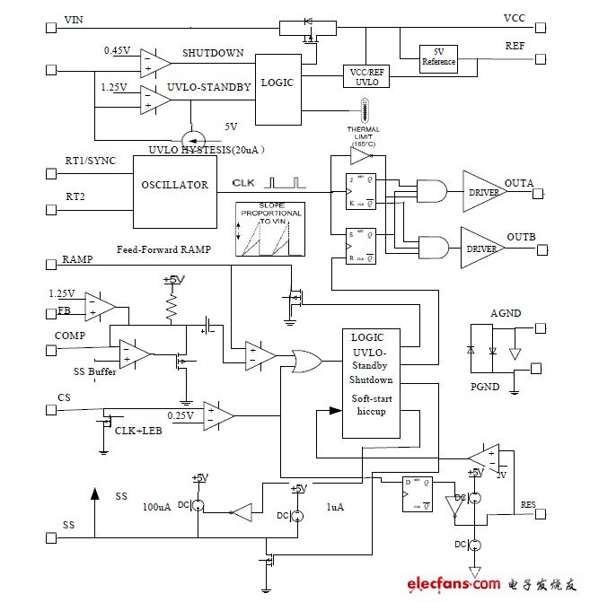
Figure 2 Internal structure of LM25037
3.1.2 DC/DC Circuit Design
The schematic diagram of the push-pull circuit controlled by LM25027 is shown in Figure 3. Its working principle is as follows: When the forward bias voltage added to the chip VIN terminal is in the range of 5~75V, the voltage reference inside the chip is established, and Vin charges the capacitor C3. At the end of each switching cycle, the internal MOS tube is turned on, C3 is discharged, and the voltage of the RAMP pin is a sawtooth wave with a slope proportional to the input voltage. The internal 1uA current source starts to charge the capacitor C10 connected to the SS pin. When the SS pin voltage reaches 1V, when the UVLO pin voltage is higher than 1.25V after R4 and R5 voltage division, the output duty cycle starts to increase from small, and the charging current becomes 100uA until the SS pin voltage reaches 5V. At the beginning of each switching cycle, there is a PWM output high. When the voltage on C3 reaches the given voltage, the PWM output is low. The internal NOR gate control logic OUTA and OUTB output alternately. R6 can set the frequency of the oscillator, and R7 can set the dead time. During the operation of the circuit, the current on the main circuit is detected in real time. When the voltage on the sampling resistor exceeds 0.25V, the output pulse is blocked. At the same time, the internal 20uA current source charges the capacitor C9 on the RES pin. When the voltage on C9 reaches 2V, C9 and C10 are discharged, and the SS terminal starts soft start. The time for the timed restart is set by the size of C9.
According to the chip data sheet, the switching frequency is set to f=51K, the dead time is 250ns, and R6=62KW and R7=3KW.
The restart time setting after overcurrent protection is shown in Figure 4.


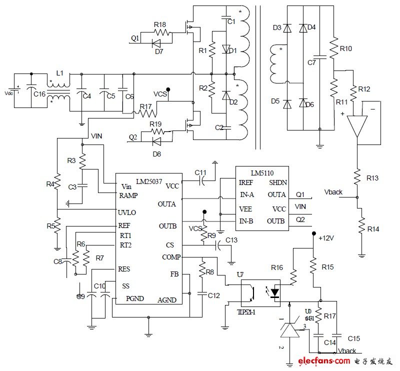
Figure 3 Push-pull circuit schematic
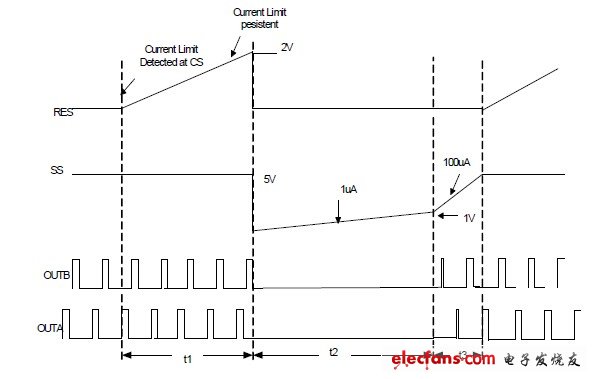
Figure 4: Timing diagram of scheduled restart.
Take C8=100pF C10=100nF, then Tres is about 10.4ms.

Among them, U1=1V, U2=5V.
The feed-forward voltage signal is charged to C by the input voltage in each switching cycle through an external RC network, and discharged to C by the MOSFET inside the chip at the end of the switching cycle to obtain a sawtooth wave proportional to the input voltage as shown in Figure 5.

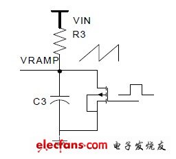
Figure 5 Voltage feed-forward network.
Take C3=100pF, R3=200KW, where Tdischarge <50nS, Tsw is the oscillation period, VRAMP is the slope voltage peak, and Vin is the input voltage.
3.2 Transformer Design
In CCM mode, the turns ratio of the transformer is mainly determined by the input voltage, output voltage and duty cycle. The minimum input voltage is Vin=9.6V. In order to prevent direct conduction, the maximum duty cycle Dmax=0.45, and the output voltage Vo=310V, then the turns ratio is:

Under the same input and output conditions, in DCM mode, the ratio of input to output voltage is not proportional to the duty cycle. The actual working duty cycle is smaller than the set value at full load. In order to improve the efficiency of the converter, the actual turn ratio is selected as n=32.
Using AP method to estimate transformer core:

Po is the output power; f is the switching frequency; Bmax is the maximum magnetic induction intensity of the transformer.
Select ferrite EE33 core AP=1.57㎝ 4 Ae=1.23㎝ 2Aw=1.27㎝ 2.
The number of turns on the original side is:

The actual number of turns for the primary side is 3 and the number of turns for the secondary side is 96.
An air gap is added when the transformer is wound. On the one hand, it is to delay the magnetic flux saturation of the push-pull circuit. On the other hand, since there is no filter inductor in the rectifier output, the actual working process uses the leakage inductance of the transformer to prevent the current peak from being too large when the switch tube is turned on. However, after adding the air gap, the leakage inductance of the transformer increases, which will increase the voltage spike, so a snubber circuit needs to be added to absorb the voltage spike.
3.3 RCD clamping circuit design
In order to reduce the turn-off voltage spike, an RCD clamp circuit connected to the positive pole of the power supply is used, as shown in Figure 6. When VT1 is turned off, D1 is turned on, and the energy on the leakage inductance is transferred to C1. The charging of C1 delays the rise of the collector voltage. The advantage of connecting R1 and D1 to Vdc is that the maximum voltage on C1 is only Vdc, instead of 2Vdc when R1 and D1 are grounded, and the voltage stress on C1 is reduced.

Figure 6 RCD snubber circuit.
Analysis of the working process of the buffer circuit:
Working mode I: As shown in Figure 7, when VT1 is turned off, the voltage of the leakage inductor Ld1 is reversed, D1 is turned on, and the capacitor C1 is charged. The voltage polarity induced on the transformer N1 is positive at the top and negative at the bottom and starts to rise. At the same time, a voltage equal to that of N1 is induced on the N2 winding of the transformer. Part of the energy on the leakage inductance is transferred to C2. The voltage on C2 changes from negative at the top and positive at the bottom to positive at the top and negative at the bottom after being charged by the transformer N2 and R2.

Figure 7 Working mode I.
Working mode II: As shown in Figure 8, after the energy on the leakage inductance is released, the energy on the excitation inductance continues to charge C1, and the voltage on the transformers N1 and N2 also increases accordingly, so the voltage on the DS terminal of VT1 increases and the voltage on the DS terminal of VT2 decreases.

Figure 8 Working mode II.
Working mode III: As shown in Figure 9, when the excitation inductance is relatively large, when the voltage on capacitor C1 is charged to the power supply voltage with positive upper and negative lower, the secondary rectifier diode is turned on, and the drain-source voltages of VT1 and VT2 are clamped at 2Vdc and 0 respectively, so the switch tube can achieve zero voltage turn-on.

Figure 9 Working mode III.
The simulation waveform of the buffer circuit is shown in Figure 10. It can be seen that the buffer circuit can achieve zero voltage turn-on.

Figure 10: Buffer circuit simulation waveform.
4. Experimental waveform
The following experimental waveforms are measured at Vin=12V full load. The switch tube drive waveform and the DS terminal waveform at full load are shown in Figures 11 and 12 respectively, the DC bus voltage and ripple are shown in Figures 13 and 14, and Figure 15 is the inverter output waveform. It can be seen that all performance indicators can be met.

Figure 11 Switch tube driving waveform at full load.

Figure 12: Voltage waveform at the DS terminal of the switch tube at full load.

Figure 13 DC bus voltage waveform.

Figure 14 DC bus ripple voltage.

Figure 15 Transformer primary current waveform.

Figure 16 Inverter output voltage waveform.
5. Conclusion
This paper proposes a design method for a vehicle-mounted inverter based on LM25037. The inverter power supply adopts integrated chip control and has the following characteristics: ① It adopts feedforward control, which has a faster dynamic response speed than the commonly used voltage control mode; ② The protection function inside the chip makes the peripheral circuit simple; ③ The inverter circuit is simple to control, with stable performance and low cost. After adding the RCD buffer circuit, the switch tube is turned on at zero voltage, and the system efficiency is improved. The experimental prototype verifies that the vehicle-mounted inverter works stably and reliably and can continuously output 150W.
Previous article:Design of AC Inverter Power Supply Based on UC2525
Next article:Active Damping Control of LCL Filtered Three-Level Grid-Connected Inverter
Recommended ReadingLatest update time:2024-11-16 20:35
- Popular Resources
- Popular amplifiers
-
 The Car Hacker\'s Handbook: A Penetration Tester\'s Guide
 -
 Three-Phase 11 kW PFC + LLC Electric Vehicle On-Board Charging (OBC) Platform User Manual (ONSEMI Semiconductor)
 -
 Lithium-ion battery system testing and evaluation
 -
 Optimal estimation theory and its applications: modeling, filtering, information fusion estimation
- MathWorks and NXP Collaborate to Launch Model-Based Design Toolbox for Battery Management Systems
- STMicroelectronics' advanced galvanically isolated gate driver STGAP3S provides flexible protection for IGBTs and SiC MOSFETs
- New diaphragm-free solid-state lithium battery technology is launched: the distance between the positive and negative electrodes is less than 0.000001 meters
- [“Source” Observe the Autumn Series] Application and testing of the next generation of semiconductor gallium oxide device photodetectors
- 采用自主设计封装,绝缘电阻显著提高!ROHM开发出更高电压xEV系统的SiC肖特基势垒二极管
- Will GaN replace SiC? PI's disruptive 1700V InnoMux2 is here to demonstrate
- From Isolation to the Third and a Half Generation: Understanding Naxinwei's Gate Driver IC in One Article
- The appeal of 48 V technology: importance, benefits and key factors in system-level applications
- Important breakthrough in recycling of used lithium-ion batteries
- Innolux's intelligent steer-by-wire solution makes cars smarter and safer
- 8051 MCU - Parity Check
- How to efficiently balance the sensitivity of tactile sensing interfaces
- What should I do if the servo motor shakes? What causes the servo motor to shake quickly?
- 【Brushless Motor】Analysis of three-phase BLDC motor and sharing of two popular development boards
- Midea Industrial Technology's subsidiaries Clou Electronics and Hekang New Energy jointly appeared at the Munich Battery Energy Storage Exhibition and Solar Energy Exhibition
- Guoxin Sichen | Application of ferroelectric memory PB85RS2MC in power battery management, with a capacity of 2M
- Analysis of common faults of frequency converter
- In a head-on competition with Qualcomm, what kind of cockpit products has Intel come up with?
- Dalian Rongke's all-vanadium liquid flow battery energy storage equipment industrialization project has entered the sprint stage before production
- Allegro MicroSystems Introduces Advanced Magnetic and Inductive Position Sensing Solutions at Electronica 2024
- Car key in the left hand, liveness detection radar in the right hand, UWB is imperative for cars!
- After a decade of rapid development, domestic CIS has entered the market
- Aegis Dagger Battery + Thor EM-i Super Hybrid, Geely New Energy has thrown out two "king bombs"
- A brief discussion on functional safety - fault, error, and failure
- In the smart car 2.0 cycle, these core industry chains are facing major opportunities!
- The United States and Japan are developing new batteries. CATL faces challenges? How should China's new energy battery industry respond?
- Murata launches high-precision 6-axis inertial sensor for automobiles
- Ford patents pre-charge alarm to help save costs and respond to emergencies
- New real-time microcontroller system from Texas Instruments enables smarter processing in automotive and industrial applications
- USB Type-C and USB Power Delivery Power Path Design Considerations
- xds510 simulator transfer
- TVS Tube
- How to detect whether two points in a circuit are short-circuited to each other?
- How to handle different tasks at the same time in the time slice polling method
- Simple voice-controlled light circuit schematic and PCB wiring method
- LPS22HH air pressure sensor PCB package and code
- Xunwei-IMX6 development board device tree-Linux kernel configuration two-way CAN
- Looking for a chip that can be used with 485 and 232
- CC2540 beginners learning how to use buttons

 The Car Hacker\'s Handbook: A Penetration Tester\'s Guide
 Three-Phase 11 kW PFC + LLC Electric Vehicle On-Board Charging (OBC) Platform User Manual (ONSEMI Semiconductor)


 京公网安备 11010802033920号