1 Introduction
The development of information technology has long penetrated into all areas of the national economy, and radar technology has played a vital role in the military field since its advent. In order to meet the observation requirements of artificial satellites and ballistic missiles, active phased array radar technology has achieved rapid development. The
T/R component beam control circuit is a key component on the active phased array radar. The beam control circuit is generally a customized dedicated chip. Different beam control circuits are quite different, but their main working principles and internal structures are roughly the same. Due to its special nature, the test of the beam control circuit is more troublesome. This paper analyzes the main internal structure of the beam control circuit, finds out the difficulties in circuit testing, proposes a solution, and gives the design principle and structure, which provides a simplified idea for the test of this type of circuit.
2 Principles and test difficulties of beam control circuits
Most of the beam control circuits are dedicated circuits, but their main principles and internal structures are roughly the same, mainly including three parts: serial-to-parallel conversion, fault detection, and control signal. Serial-to-parallel conversion converts multi-bit serial data into parallel data, which is driven and output, followed by component phase shifters and attenuators. Due to different user needs, the number of serial data bits varies greatly, ranging from 26 bits to 50 bits and even higher. Fault detection is mainly used to realize parity verification and parallel-serial conversion output. Some beam control circuits also have some analog detection functions, such as undervoltage protection. The control signal part is mainly some logic function signals, which are used for component control signals. Therefore, the beam control circuit can be said to be a digital analog integrated circuit that integrates sequential logic and combinational logic .
Figures 1 and 2 respectively show the working principle and timing of a beam control circuit, and its internal structure includes the above three parts. It can be seen that the test difficulties of the beam control circuit are as follows:
1) There are many input signals, and there is a strict timing relationship between the input signals, which is the characteristic of digital circuits;
2) There are many output signals, including positive power supply output and negative power supply output, and the negative level voltage of the wave control output is incompatible with many large test equipment interfaces;
3) The logical combination relationship is relatively complex, and a large amount of vector storage space is required during testing;
4) The test of the self-test signal is not easy to handle.
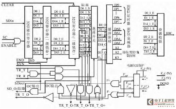
Figure 1 Working principle of beam control circuit
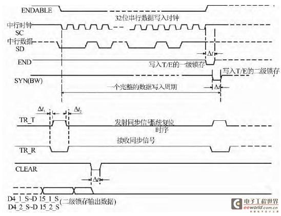
Figure 2 Working sequence of beam control circuit
3 Test solution
Figure 3 shows the test solution proposed in this paper. To solve the problem that there are many input signals of the beam control circuit and there is a strict timing relationship between the input signals, programmable devices (such as FPGA , CPLD ) can be used to generate the required signals. Since the input high and low level voltages need to be strictly controlled when testing the beam control circuit, those circuits with defective input flip levels caused by the process manufacturing process are removed during the test screening. The output of the programmable device cannot be directly transmitted to the device under test. A level conversion drive circuit needs to be added to meet the input test requirements of the beam control circuit.
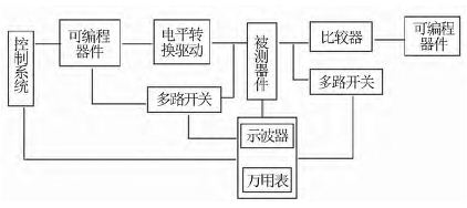
Figure 3 Test solution for beam control circuit
The most important parameter in the beam control circuit is the result of the functional test. Due to the large number of output channels, complex logical relationships, and large number of test vectors, it is impossible to exhaust all logical relationships during the test. In actual testing, partial truth tables are often used as the basis for functional judgment. Table 1 is a common truth table of a beam control circuit. This table format is convenient for test judgment.
Table 1 Truth table of beam control circuit

Obviously, the best way to judge this kind of logical relationship is to use field programmable devices. Programmable devices have more IO resources, and have a certain amount of internal storage space. They can also perform logical operations to improve test efficiency.
Generally speaking, the output of the beam control circuit is incompatible with the programmable device and cannot be directly connected, so it is necessary to choose a way to solve the problem of level incompatibility. There are two relatively simple ways: one is to use a resistor network, and the other is to use a level conversion interface chip. These two methods have their own advantages and disadvantages: the resistor network structure is simple and low cost, but the flexibility is poor; the level conversion interface chip is relatively complex and the cost is correspondingly higher, but the design is flexible.
This article recommends the second method, because the output mode of the beam control chip is likely to be many, such as 0~-5V output, or 0~5V output, or both. Using a comparator to achieve level conversion is a better choice.
As for the judgment of time parameters and some static parameters, they can be directly tested through a GPIB programmable oscilloscope and a digital multimeter to ensure the test accuracy of the parameters.
4 Design Example
In the experiment, the input signal channel is preset to 16 bits, the frequency range is 0~40MHz, the input level range is -5~8V adjustable, and the output signal channel is 64 bits optional, which can meet the test requirements of most conventional wave control circuits.
4.1 Drive Circuit
The drive circuit uses Intersil 's EL7457, which has a maximum drive capacity of 2A, 4 inputs and 4 outputs, and a maximum frequency of 40MHz. The output high level range is -2~16.5V, and the output low level range is -5~8V, which fully meets the input requirements of conventional wave control circuits. The principle of the drive circuit is shown in Figure 4, where R1~R4 are small resistors connected in series to reduce the overshoot of the output waveform, and L and H are the set output high and low level values. The advantage of this design is that the input high and low levels are adjustable and do not affect the input timing.
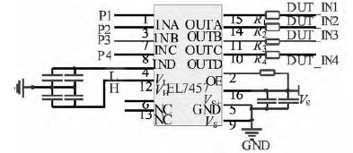
Figure 4 Driving circuit principle
4.2 Comparator
The comparator uses a high-speed, low-voltage difference comparator MAX901 launched by Maxim . It can be powered by dual power supplies or single power supplies, and the output voltage can be set according to user requirements. The circuit peripheral design is shown in Figure 5. CHV is the comparison voltage setting, CH1~CH4 is the output port of the device under test, and FCH1~FCH4 is the FPGA receiving port. By setting the MAX901 comparison voltage, the logical function of the device at different voltage outputs can be tested. The function of D1~D4 is to indicate and facilitate debugging. [page]
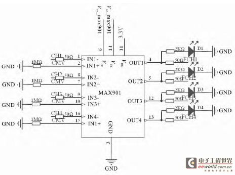
Figure 5 Comparator circuit principle
4.3 Programmable part
The programmable device uses a low-end product XC3S50AN from Xilinx . This is because only rich IO resources and vector storage are used in the test. There is no high requirement, so it is enough to use a low-end product. Figure 6 shows the configuration of JTAG for FPGA program download. The power module circuit principle is shown in Figure 7. Only two power supplies are required, the core is 1.2V, and the auxiliary voltage and port voltage are set to 3.3V.
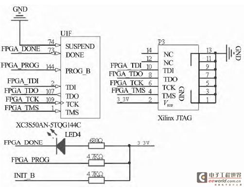
Figure 6 JTAG configuration
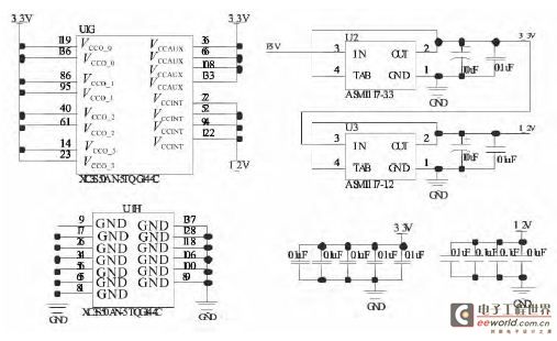
Figure 7 Power module circuit principle
Timing simulationTwo programmable devices can be used, one for data transmission and switch control, and the other for data reception and function judgment. Figure 8 shows the simulation waveform of the data transmission FPGA, S is the FPGA output switch control signal; delay_sn, delay_clk, delay_clr are the switch control input signals, which realize the parallel output of serial data; P is the signal output by FPGA to the device under test, which is controlled by dutin_r, dutin_s, dutin_clk, dutin_clr, IN. It can be seen that using FPGA to generate timing is a more ideal choice.

Figure 8 Input timing simulation
Figure 9 shows the data reception FPGA simulation waveform. CH receives and stores the logic value of the device under test, datain, dataclk, address are used to set the ideal logic value. PASS, FAIL are output status indications.

Figure 9 Function judgment simulation
4.4 Test results
Figure 10 shows a photo of the wave control circuit test system made according to the scheme of this article. The upper left picture shows two FPGAs, one for data transmission and the other for data reception judgment; the upper right picture shows the system power module, and the lower picture shows the system combination. The system can realize full parameter test of conventional beam control circuit with input within 16 bits and output within 64 bits. Table 2 lists the measured results of a 32-bit T/R component beam control circuit. Among them, the comparison level of the comparator is set to 4.8V and 0.2V, so the output high level is ≥4.8V and the low level is ≤0.2V.
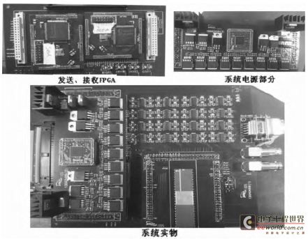
Figure 10 Actual photo of the beam control circuit test system
Table 2 Test results

5 Conclusion
Beam control circuits are highly specialized, have many input and output interfaces, strict timing, and complex logical functions, so their testing is relatively complex. This paper proposes a test scheme. The scheme is simple and easy to implement. It makes full use of the rich IO resources and programmable characteristics of FPGA, and solves the difficulties in beam control circuit testing. At the same time, this method is easy to realize the versatility of conventional wave control circuit test systems. It only needs to define the input interface of the test system transfer part and write different sending and receiving programs to realize the versatility of conventional wave control circuits.
Reference address:Design of T/R module beam steering test solution
The development of information technology has long penetrated into all areas of the national economy, and radar technology has played a vital role in the military field since its advent. In order to meet the observation requirements of artificial satellites and ballistic missiles, active phased array radar technology has achieved rapid development. The
T/R component beam control circuit is a key component on the active phased array radar. The beam control circuit is generally a customized dedicated chip. Different beam control circuits are quite different, but their main working principles and internal structures are roughly the same. Due to its special nature, the test of the beam control circuit is more troublesome. This paper analyzes the main internal structure of the beam control circuit, finds out the difficulties in circuit testing, proposes a solution, and gives the design principle and structure, which provides a simplified idea for the test of this type of circuit.
2 Principles and test difficulties of beam control circuits
Most of the beam control circuits are dedicated circuits, but their main principles and internal structures are roughly the same, mainly including three parts: serial-to-parallel conversion, fault detection, and control signal. Serial-to-parallel conversion converts multi-bit serial data into parallel data, which is driven and output, followed by component phase shifters and attenuators. Due to different user needs, the number of serial data bits varies greatly, ranging from 26 bits to 50 bits and even higher. Fault detection is mainly used to realize parity verification and parallel-serial conversion output. Some beam control circuits also have some analog detection functions, such as undervoltage protection. The control signal part is mainly some logic function signals, which are used for component control signals. Therefore, the beam control circuit can be said to be a digital analog integrated circuit that integrates sequential logic and combinational logic .
Figures 1 and 2 respectively show the working principle and timing of a beam control circuit, and its internal structure includes the above three parts. It can be seen that the test difficulties of the beam control circuit are as follows:
1) There are many input signals, and there is a strict timing relationship between the input signals, which is the characteristic of digital circuits;
2) There are many output signals, including positive power supply output and negative power supply output, and the negative level voltage of the wave control output is incompatible with many large test equipment interfaces;
3) The logical combination relationship is relatively complex, and a large amount of vector storage space is required during testing;
4) The test of the self-test signal is not easy to handle.

Figure 1 Working principle of beam control circuit

Figure 2 Working sequence of beam control circuit
3 Test solution
Figure 3 shows the test solution proposed in this paper. To solve the problem that there are many input signals of the beam control circuit and there is a strict timing relationship between the input signals, programmable devices (such as FPGA , CPLD ) can be used to generate the required signals. Since the input high and low level voltages need to be strictly controlled when testing the beam control circuit, those circuits with defective input flip levels caused by the process manufacturing process are removed during the test screening. The output of the programmable device cannot be directly transmitted to the device under test. A level conversion drive circuit needs to be added to meet the input test requirements of the beam control circuit.

Figure 3 Test solution for beam control circuit
The most important parameter in the beam control circuit is the result of the functional test. Due to the large number of output channels, complex logical relationships, and large number of test vectors, it is impossible to exhaust all logical relationships during the test. In actual testing, partial truth tables are often used as the basis for functional judgment. Table 1 is a common truth table of a beam control circuit. This table format is convenient for test judgment.
Table 1 Truth table of beam control circuit

Obviously, the best way to judge this kind of logical relationship is to use field programmable devices. Programmable devices have more IO resources, and have a certain amount of internal storage space. They can also perform logical operations to improve test efficiency.
Generally speaking, the output of the beam control circuit is incompatible with the programmable device and cannot be directly connected, so it is necessary to choose a way to solve the problem of level incompatibility. There are two relatively simple ways: one is to use a resistor network, and the other is to use a level conversion interface chip. These two methods have their own advantages and disadvantages: the resistor network structure is simple and low cost, but the flexibility is poor; the level conversion interface chip is relatively complex and the cost is correspondingly higher, but the design is flexible.
This article recommends the second method, because the output mode of the beam control chip is likely to be many, such as 0~-5V output, or 0~5V output, or both. Using a comparator to achieve level conversion is a better choice.
As for the judgment of time parameters and some static parameters, they can be directly tested through a GPIB programmable oscilloscope and a digital multimeter to ensure the test accuracy of the parameters.
4 Design Example
In the experiment, the input signal channel is preset to 16 bits, the frequency range is 0~40MHz, the input level range is -5~8V adjustable, and the output signal channel is 64 bits optional, which can meet the test requirements of most conventional wave control circuits.
4.1 Drive Circuit
The drive circuit uses Intersil 's EL7457, which has a maximum drive capacity of 2A, 4 inputs and 4 outputs, and a maximum frequency of 40MHz. The output high level range is -2~16.5V, and the output low level range is -5~8V, which fully meets the input requirements of conventional wave control circuits. The principle of the drive circuit is shown in Figure 4, where R1~R4 are small resistors connected in series to reduce the overshoot of the output waveform, and L and H are the set output high and low level values. The advantage of this design is that the input high and low levels are adjustable and do not affect the input timing.

Figure 4 Driving circuit principle
4.2 Comparator
The comparator uses a high-speed, low-voltage difference comparator MAX901 launched by Maxim . It can be powered by dual power supplies or single power supplies, and the output voltage can be set according to user requirements. The circuit peripheral design is shown in Figure 5. CHV is the comparison voltage setting, CH1~CH4 is the output port of the device under test, and FCH1~FCH4 is the FPGA receiving port. By setting the MAX901 comparison voltage, the logical function of the device at different voltage outputs can be tested. The function of D1~D4 is to indicate and facilitate debugging. [page]

Figure 5 Comparator circuit principle
4.3 Programmable part
The programmable device uses a low-end product XC3S50AN from Xilinx . This is because only rich IO resources and vector storage are used in the test. There is no high requirement, so it is enough to use a low-end product. Figure 6 shows the configuration of JTAG for FPGA program download. The power module circuit principle is shown in Figure 7. Only two power supplies are required, the core is 1.2V, and the auxiliary voltage and port voltage are set to 3.3V.

Figure 6 JTAG configuration

Figure 7 Power module circuit principle
Timing simulationTwo programmable devices can be used, one for data transmission and switch control, and the other for data reception and function judgment. Figure 8 shows the simulation waveform of the data transmission FPGA, S is the FPGA output switch control signal; delay_sn, delay_clk, delay_clr are the switch control input signals, which realize the parallel output of serial data; P is the signal output by FPGA to the device under test, which is controlled by dutin_r, dutin_s, dutin_clk, dutin_clr, IN. It can be seen that using FPGA to generate timing is a more ideal choice.

Figure 8 Input timing simulation
Figure 9 shows the data reception FPGA simulation waveform. CH receives and stores the logic value of the device under test, datain, dataclk, address are used to set the ideal logic value. PASS, FAIL are output status indications.

Figure 9 Function judgment simulation
4.4 Test results
Figure 10 shows a photo of the wave control circuit test system made according to the scheme of this article. The upper left picture shows two FPGAs, one for data transmission and the other for data reception judgment; the upper right picture shows the system power module, and the lower picture shows the system combination. The system can realize full parameter test of conventional beam control circuit with input within 16 bits and output within 64 bits. Table 2 lists the measured results of a 32-bit T/R component beam control circuit. Among them, the comparison level of the comparator is set to 4.8V and 0.2V, so the output high level is ≥4.8V and the low level is ≤0.2V.

Figure 10 Actual photo of the beam control circuit test system
Table 2 Test results

5 Conclusion
Beam control circuits are highly specialized, have many input and output interfaces, strict timing, and complex logical functions, so their testing is relatively complex. This paper proposes a test scheme. The scheme is simple and easy to implement. It makes full use of the rich IO resources and programmable characteristics of FPGA, and solves the difficulties in beam control circuit testing. At the same time, this method is easy to realize the versatility of conventional wave control circuit test systems. It only needs to define the input interface of the test system transfer part and write different sending and receiving programs to realize the versatility of conventional wave control circuits.
Previous article:Three Typical Methods for Noise Figure Measurement
Next article:Measurement of non-intrusive devices
Recommended Content
Latest Test Measurement Articles
- Keysight Technologies Helps Samsung Electronics Successfully Validate FiRa® 2.0 Safe Distance Measurement Test Case
- From probes to power supplies, Tektronix is leading the way in comprehensive innovation in power electronics testing
- Seizing the Opportunities in the Chinese Application Market: NI's Challenges and Answers
- Tektronix Launches Breakthrough Power Measurement Tools to Accelerate Innovation as Global Electrification Accelerates
- Not all oscilloscopes are created equal: Why ADCs and low noise floor matter
- Enable TekHSI high-speed interface function to accelerate the remote transmission of waveform data
- How to measure the quality of soft start thyristor
- How to use a multimeter to judge whether a soft starter is good or bad
- What are the advantages and disadvantages of non-contact temperature sensors?
MoreSelected Circuit Diagrams
MorePopular Articles
- Innolux's intelligent steer-by-wire solution makes cars smarter and safer
- 8051 MCU - Parity Check
- How to efficiently balance the sensitivity of tactile sensing interfaces
- What should I do if the servo motor shakes? What causes the servo motor to shake quickly?
- 【Brushless Motor】Analysis of three-phase BLDC motor and sharing of two popular development boards
- Midea Industrial Technology's subsidiaries Clou Electronics and Hekang New Energy jointly appeared at the Munich Battery Energy Storage Exhibition and Solar Energy Exhibition
- Guoxin Sichen | Application of ferroelectric memory PB85RS2MC in power battery management, with a capacity of 2M
- Analysis of common faults of frequency converter
- In a head-on competition with Qualcomm, what kind of cockpit products has Intel come up with?
- Dalian Rongke's all-vanadium liquid flow battery energy storage equipment industrialization project has entered the sprint stage before production
MoreDaily News
- Allegro MicroSystems Introduces Advanced Magnetic and Inductive Position Sensing Solutions at Electronica 2024
- Car key in the left hand, liveness detection radar in the right hand, UWB is imperative for cars!
- After a decade of rapid development, domestic CIS has entered the market
- Aegis Dagger Battery + Thor EM-i Super Hybrid, Geely New Energy has thrown out two "king bombs"
- A brief discussion on functional safety - fault, error, and failure
- In the smart car 2.0 cycle, these core industry chains are facing major opportunities!
- The United States and Japan are developing new batteries. CATL faces challenges? How should China's new energy battery industry respond?
- Murata launches high-precision 6-axis inertial sensor for automobiles
- Ford patents pre-charge alarm to help save costs and respond to emergencies
- New real-time microcontroller system from Texas Instruments enables smarter processing in automotive and industrial applications
Guess you like
- Radio beacon-guided drones can detect toxic gases
- EEWORLD University Hall - Planting the latest and hottest LED driver products from TI
- CC3200 LaunchPad Out of Box Test demos-appliances
- How should a novice in digital circuits save himself?
- TI Battery Fuel Gauging Basics Training
- 【ST NUCLEO-H743ZI Review】(5) USB to Serial
- EEWORLD University ---- Haiwell IoT Terminal MQTT Protocol Application Video Tutorial
- [TI mmWave Radar Review] Introduction to Sensor Management Module
- Survival rules for electronic engineers in the workplace, every word is true!
- 【XMC4800 Relax EtherCAT Kit Review】+ Getting Started with DAVE, Modbus Bus Comprehensive Application

 Offline (Non-Isolated) AC/DC Power Supply Architecture Reference Design for Grid Applications


 京公网安备 11010802033920号