introduction
As devices continue to miniaturize, semiconductor device reliability testing and device lifetime prediction face great challenges. Due to the increasing complexity of new materials and new processes, the randomness of device failures is also increasing. 1 This requires the generation of larger statistical sample test data. Although traditional stress-switch-measure reliability testing techniques can achieve a large number of device tests, this approach can be problematic. Using TDDB, engineers need to monitor soft breakdown and progressive breakdown. With NBTI, device relaxation must be minimized and measurements must be completed at extremely fast speeds. At the level of testing individual devices, some issues are still controllable, but sequentially testing individual devices over a practical period of time does not provide a large number of statistical sample data.
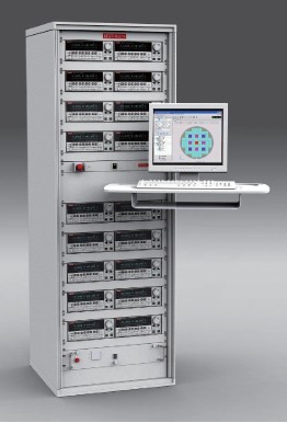
Figure 1. Example of an ACS Integrated Test System Using an SMU -per-pin Architecture
This application note discusses how to overcome reliability test challenges with an ACS integrated test system and SMU (source-measure unit)-per-pin configuration. Using Keithley Series 2600 SourceMeter and Automated Characterization Suite (ACS) software, medium-sized systems (20-40 pins) can be implemented for increasingly complex tests such as TDDB, NBTI, and HCI. High-throughput testing is possible due to the fully automated probe control and automated test sequencing capabilities included in ACS. The SMU-per-pin configuration also plays an important role in providing system flexibility and ease of use after eliminating switches. In addition, ACS provides an integrated test flow environment, convenient point-and-click operation, and includes common reliability tests such as: • TDDB, Vramp, JRamp (JEDEC standard test) • HCI (NBTI), Instant NBTI, NBTI Fast SMU • EM, Isothermal EM (JEDEC standard test) Users can use the modules of the standard library as templates to quickly develop their own tests with ACS. Figure 2 shows an example of TDDB testing with ACS.
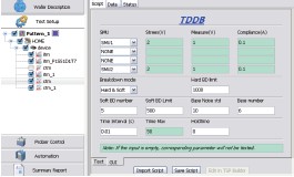
SMU-Per-Pin WLR Test
The concept of SMU-per-pin is simple - remove the switch matrix from the system architecture and replace the missing pin connections with independent SMUs. Use the innovative TSP-LinkTM to connect several Series 2600 instruments to operate as a single instrument. To better understand the advantages of the SMU-per-pin architecture, consider the following two scenarios. • Testing a common pin structure • Testing the reliability of several devices at the same time
Common pad/pin test structure
Consider the shared pin device of Figure 3. Four MOSFETs share common gate and substrate pin connections, and each MOSFET has separate drain and source pin connections. A shared SMU configuration allows the devices to be tested sequentially using four SMUs and a switch matrix. By partitioning the structure into several smaller devices, the test time is increased due to switching. In addition, degradation recovery occurs during the switching process in most reliability tests, which changes the measured degradation and subsequent lifetime prediction. The shared SMU architecture in this case has another disadvantage. While measuring one device, the remaining devices are affected by the gate voltage changes. This can introduce undesirable changes in gate stress. The SMU-per-pin architecture has the significant advantage of eliminating switching delays and enabling parallel testing without driving the gate of each structure.
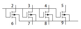
Figure 4 shows the shared SMU and SMU-per-pin configurations for a multi-device TDDB test structure. In the switched (shared SMU) case, SMU1 provides continuous stress to all structures in the test sequence, and SMU2 measures each device sequentially. In the process of analyzing the structures sequentially, the switching delays and limited measurement speed combine to limit the measurement speed of each structure. Therefore, these delays must be analyzed and converted into life analysis to ensure accurate life estimates. Moreover, if one structure suffers a catastrophic failure, other structures in the group will suffer voltage transients, temporarily lose stress conditions and may make the measurement results inaccurate. The SMU-per-pin architecture is not affected by switching delays and poor structural connections, but more importantly, the measurement speed is very fast, which is critical for acquiring high-speed progressive breakdown phenomena. [page]
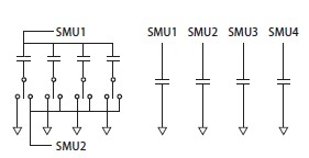
Figure 4. TDDB testing using a shared SMU architecture on the left and an SMU-per-pin architecture on the right.
NBTI testing presents different issues. The NBTI test structure is a MOSFET where stress is applied to the gate and measured at the drain, with the source and substrate grounded. NBTI requires very high measurement speeds due to degradation recovery issues. The stress interruption time for characterization should be kept as short as possible. The faster the measurement speed, the more accurate the degradation measurement. 2 Obviously, a shared SMU system introduces a delay between the stress and measurement cycles, and introduces variability in the stress duration between characterizations. Even when using potentially damaging thermal switching techniques3, variations in stress cycle lengths must be measured and accounted for during lifetime analysis.
Parallel testing and multiple groups of parallel testing improve the utilization of testers and probes and increase throughput by measuring multiple devices simultaneously. The increased throughput can be several times that of the sequential test flow shown in Figure 5 relative to standard reliability testing.
For simple tests consisting of only stress-measure sequences, a shared SMU approach can reduce test time with faster sources, shorter settling delays, and higher integration rates. This comes at the high cost of increased measurement error. Another parallel testing approach can provide test results for four devices in the time it previously took to test one. Of course, this assumes that the test time is much longer than the overhead (e.g., probe movement). Increasing the number of devices under test, especially in longer reliability tests, can save significant time and provide more statistical data samples.
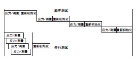
Figure 5. Time difference between sequential and parallel testing
Implementation of Parallel SMU-per-pin ACS Integrated Test System
Using multiple GPIB groups of Series 2600 SourceMeters enables parallel testing of the ACS integrated test system. Typically, a group of 4 SMUs (2 Series 2600 instruments) is used to measure a 4-terminal FET or 4 capacitors. The Series 2600 instruments in the group are connected using TSP-LinkTM and controlled as a single instrument. This approach enables system scalability and simplifies test management within the ACS. Therefore, multiple groups of SMU-per-pin test systems can be established. For parallel testing, the test script is preloaded into each 2600 host and saved in its memory. When triggered, the controller will initiate a function call to each group's host, which will run the script to coordinate the other 2600 instruments. The controller then scans the bus and receives test results from the 2600 host.
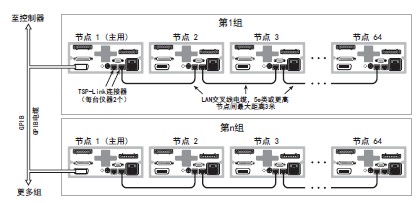
Figure 6. Example of a setup for multiple groups of Series 2600 instruments connected using GPIB and TSP-Link. Each group starts running a script (same or different) at the same time.
in conclusion
Increased time-to-market and test cost pressures mean test engineers must do more with less. Leveraging Keithley's proven instruments and measurements, the ACS Integrated Test System fills the gap between interactive lab-based tools and high-throughput production test tools. The ACS system shown in Figure 1 represents an SMU-per-pin configuration that is very beneficial for miniaturized CMOS reliability testing. Engineers using this system have great system flexibility and throughput, providing not only a huge amount of statistical data, but also excellent performance of individual device measurements.
Previous article:PCIe 3.0 Receiver Physical Layer Test Solution
Next article:Jitter and Timing Analysis in the Presence of Crosstalk
Recommended ReadingLatest update time:2024-11-16 13:24
- Keysight Technologies Helps Samsung Electronics Successfully Validate FiRa® 2.0 Safe Distance Measurement Test Case
- From probes to power supplies, Tektronix is leading the way in comprehensive innovation in power electronics testing
- Seizing the Opportunities in the Chinese Application Market: NI's Challenges and Answers
- Tektronix Launches Breakthrough Power Measurement Tools to Accelerate Innovation as Global Electrification Accelerates
- Not all oscilloscopes are created equal: Why ADCs and low noise floor matter
- Enable TekHSI high-speed interface function to accelerate the remote transmission of waveform data
- How to measure the quality of soft start thyristor
- How to use a multimeter to judge whether a soft starter is good or bad
- What are the advantages and disadvantages of non-contact temperature sensors?
- Innolux's intelligent steer-by-wire solution makes cars smarter and safer
- 8051 MCU - Parity Check
- How to efficiently balance the sensitivity of tactile sensing interfaces
- What should I do if the servo motor shakes? What causes the servo motor to shake quickly?
- 【Brushless Motor】Analysis of three-phase BLDC motor and sharing of two popular development boards
- Midea Industrial Technology's subsidiaries Clou Electronics and Hekang New Energy jointly appeared at the Munich Battery Energy Storage Exhibition and Solar Energy Exhibition
- Guoxin Sichen | Application of ferroelectric memory PB85RS2MC in power battery management, with a capacity of 2M
- Analysis of common faults of frequency converter
- In a head-on competition with Qualcomm, what kind of cockpit products has Intel come up with?
- Dalian Rongke's all-vanadium liquid flow battery energy storage equipment industrialization project has entered the sprint stage before production
- Allegro MicroSystems Introduces Advanced Magnetic and Inductive Position Sensing Solutions at Electronica 2024
- Car key in the left hand, liveness detection radar in the right hand, UWB is imperative for cars!
- After a decade of rapid development, domestic CIS has entered the market
- Aegis Dagger Battery + Thor EM-i Super Hybrid, Geely New Energy has thrown out two "king bombs"
- A brief discussion on functional safety - fault, error, and failure
- In the smart car 2.0 cycle, these core industry chains are facing major opportunities!
- The United States and Japan are developing new batteries. CATL faces challenges? How should China's new energy battery industry respond?
- Murata launches high-precision 6-axis inertial sensor for automobiles
- Ford patents pre-charge alarm to help save costs and respond to emergencies
- New real-time microcontroller system from Texas Instruments enables smarter processing in automotive and industrial applications
- A troubleshooting example of connecting XDS100V3 debugging target board with CCS
- 【Android Development Learning Road】Part 2-- HelloEEWorld
- 51 MCU library serial port sends a segment of characters and the digital tube receives and displays them (use the serial port debugging assistant to modify the data)
- pic18F27Q10 eeprom erase problem
- 【BearPi-HM Micro】Part 4: Familiar with the Openharmomy compilation framework and serial port interactive output
- 50 ways to use TI CC6678 digital signal processor (DSP)
- Definition of Direct Current and Alternating Current
- [Reference Book] PCB Design Tips (ADI Think Tank)
- Share: How to reduce EMI and shrink power supply size with integrated active EMI filters
- Calculation and setting of baud rate of msp430 microcontroller

 Real-time driver monitoring system via modal and viewpoint analysis
 ICCV2023 Paper Summary: Recognition: Categorization


 京公网安备 11010802033920号