Test buses have developed rapidly in recent decades: from the early general purpose interface bus GPIB to the recent VXI, Peripheral Component Interconnection (PCI), PXI, IEEE1394, and Universal Serial Bus (USB) test buses. Among them, the PXI bus is the latest generation of test bus technology, which is an extension of the PCI bus in the test field (PCI eXtensions for Instruments). It was first proposed by the American NI company in 1997 and adopted as an industrial standard the following year. PXI bus can be simply considered as a combination of Microsoft Windows, Compact PCI (CPCI) and VXI technology: the core technology of CPCI is adopted in mechanical specifications, namely the European card mechanical mechanism and airtight pinhole connector, which is particularly suitable for harsh industrial environments; the electrical specifications add a dedicated system reference clock, trigger bus, star trigger bus and local bus between modules while maintaining all the advantages of PCI/CPCI bus, so as to meet the requirements of high-precision timing, synchronization and data communication; the software specifications are also consistent with PCI/CPCI, and the core is Microsoft's Windows operating system, so the PXI system is compatible with PC, which is convenient for choosing many ready-made application software development tools. The PXI bus system combines the advantages of PC performance and price, CPCI's superior mechanical properties and VXI's easy system integration, so it is the fastest-growing bus technology today. So far, dozens of companies such as NI in the United States have launched thousands of PXI (CPCI) modules. Based on this, this paper adopts PXI bus, uses existing PXI industrial computers and high-speed data acquisition boards, and designs virtual digital storage oscilloscope software based on PXI bus.
Hardware and software structure of digital oscilloscope based on PXI bus
Hardware structure
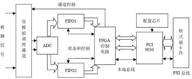
Digital oscilloscope hardware is commonly referred to as data acquisition board, and its principle block diagram is shown in Figure 1 (power supply and clock parts are omitted in the figure): The dual-channel measured signal is sent to the high-speed analog-to-digital converter through the analog signal conditioning channel, and the obtained digital data is first sent to two first-in first-out (FIFO) buffers and then sent to the local total current. Finally, it is sent to the PXI chassis by the interface chip PCI9030. The control and status reading of the hardware needs to be completed by the corresponding software according to the user's instructions. The data sent to the PXI industrial computer must also be processed by the software, and finally the display waveform and measurement results are obtained. 
Figure 1 Principle block diagram of PXI data acquisition board
Software composition
In order to ensure the security, stability and portability of the system, the Windows system has taken shielding measures for the underlying system operations, and uses device drivers to separate the hardware from the user. Therefore, the software is divided into two parts: the underlying device driver and the high-level application software. In a broad sense, the device driver refers to a set of functions that directly operate the hardware to complete hardware control and data acquisition. After loading, the driver becomes part of the operating system kernel. The high-level application software can be considered as a user-mode program of a virtual oscilloscope, which links the user interface, i.e., various switches, buttons and other controls on the panel, as well as the waveform and measurement data result display area, with data acquisition and data analysis. When the user issues a certain command on the interface, the application first calls the application programming interface (API) function, and the relevant system service will call the kernel mode driver to implement the API, convert the command information into a data format recognized by the data acquisition board, and send it to the underlying hardware according to the physical address of the data acquisition board. At the same time, the data collected by the data acquisition board and various status information of the underlying hardware are also transmitted to the application through the API for display and control.
Driver Development
Windows driver compilation can use the Windows Device Driver Development Kit (Device Drivers Kit, DDK), but programmers need to understand the complex operating system kernel. The simple method is to use KRFTech's device driver development tool WinDriver. WinDriver is a toolkit mainly used to write hardware device drivers for ISA/PCI cards and USB. For hardware access, the application calls the WinDriver function interface from the WinDriver user mode library, and then this function calls the WinDriver kernel module, that is, the drivers WinDriver.vxd and WinDriver.sys provided by WinDriver itself to complete the hardware access.
By analyzing the data acquisition board, we know that the basic functions that the driver needs to complete include device initialization, reading and writing I/O and memory, direct memory access (DMA) and interrupt operations. First, use WinDriver to complete the hardware diagnosis operation and obtain the data acquisition board hardware parameters, such as port address range, I/O mode, memory address, memory mapping mode, interrupt number, etc. Then some source code and framework functions are generated according to these hardware parameters, such as:
SHBK_HANDLE SHBK_LocateAndOpenBoard(DWORD dwVendorID,DWORD dwDeviceID,BOOL
fUseInt)//Locate and open the data acquisition board;
void SHBK_EnableDisableInterrupts(SHBK_HANDLE hSHBK)//Define to enable or disable interrupts;
DWORD SHBK_ReadPCIReg(SHBK_HANDLE hSHBK, DWORD dwReg)//Read configuration register;
BYTE SHBK_ReadByte (SHBK_HANDLE hSHBK, SHBK_ADDR addrSpace, DWORD dwOffset)//Read 1 byte of memory content, the memory address is the base address plus the offset dwOffset;
void SHBK_WriteByte (SHBK_HANDLE hSHBK, SHBK_ADDR addrSpace, DWORD dwOffset, BYTE
data) // Write 1 byte of data to the memory.
Due to space limitations, only a small number of functions are given as examples, and no specific implementation code is given for all functions. All these framework functions can be used to directly operate the hardware. In order to facilitate multiple functions to reference them, they are encapsulated in a dynamic link library (Down-Line Load, DLL), and then called according to the actual hardware design. By performing specific read and write operations on the memory and IO, function functions that operate the data acquisition board hardware are compiled. These function functions are also encapsulated in this DLL and provided for high-level application software to call. [page]
Virtual digital oscilloscope application software design
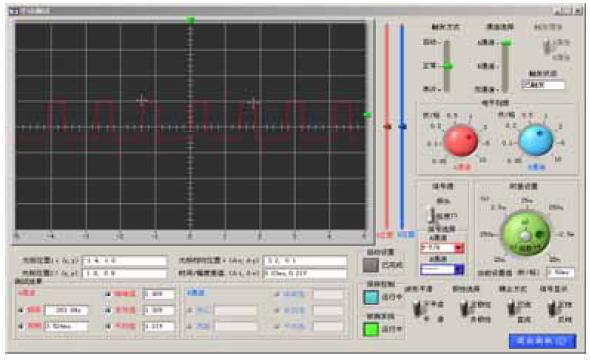
LabWindows/CVI is a C language-based software development platform developed by NI. The selection of LabWindows/CVI for virtual oscilloscope development is mainly based on the fact that LabWindows/CVI is suitable for the development of various test, control, fault analysis and information processing software, especially large and complex test software. Using LabWindows/CVI development can obtain excellent test performance [3]. For the convenience of users, the oscilloscope panel is designed to be used in the same way as a general oscilloscope. All operations are similar to those of a general oscilloscope, as shown in Figure 2. It includes the following contents:
(1) Control setting area: Users can control the corresponding controls to set the time base, range, measurement channel, trigger mode, trigger polarity, trigger level, trigger position, trigger channel, coupling mode, and whether to display the waveform smoothly and inverted. In addition, there is a special automatic setting button. Press this button and the software will automatically set the above parameters for the user.
(2) Waveform display area: The upper left part of the soft panel is divided into 10 grids horizontally and 8 grids vertically according to the standard oscilloscope display specifications; there are two movable cursors that can be dragged by the user in the waveform display area. 
Figure 2 Oscilloscope panel
(3) Cursor and measurement result display area: The positions of cursors 1 and 2, the relative positions of cursors and the corresponding time/amplitude differences can be displayed respectively. In addition, the five values of the measured signal, namely, the period, frequency, peak-to-peak value, effective value and average value, are also displayed.
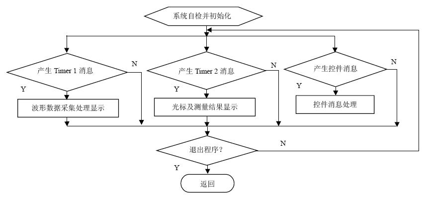
The overall module of the entire system software is shown in Figure 3, which mainly includes: initialization module, end program module, control message processing module, waveform data acquisition processing display module, cursor and measurement result display module. Strictly speaking, the latter two software modules also belong to a special control message processing. In CVI, there is a special control called a timer, which is hidden in the user interface. It continuously generates messages according to the preset time interval, and uses its message callback function to process the code that needs to be executed repeatedly. The waveform acquisition processing display program and the data display program are executed in a 20 ms and 1.2 s cycle respectively. While executing these two parts of the loop program, if there are controls on the oscilloscope panel being operated, the application will process the control message between the two cycles, and if necessary, it will call the underlying driver to set the hardware accordingly. For example, when the user changes the range control gear position through the mouse, the processing of the control message is to set the corresponding attenuation rate on the analog conditioning channel on the data acquisition board according to the changed range gear position. The initialization module includes locating and starting the data acquisition board, initializing the user interface and setting the corresponding initial hardware parameters, and then starting to collect data. In addition, there is a special button "Exit Program" in the lower right corner of the soft panel. Pressing it ends the above cycle and exits the application. 
Figure 3 General program block diagram
To complete the oscilloscope function shown in Figure 2 and finally display the waveform and data, waveform data acquisition, processing and display are the most important processes. When the "RUN/STOP" key on the panel is in the "RUN" state, the driver is called to start the data acquisition process. First, different data acquisition methods should be selected according to the different trigger channels and trigger modes. At the same time, the measured data of different time periods should be collected according to the different trigger levels and trigger positions set by the user. Before the obtained data is sent for display, the collected waveform data may also undergo certain processing as needed, such as smoothing, interpolation, anti-shake, etc. Due to the digital storage function and real-time sampling characteristics of the oscilloscope, as well as its single trigger, rolling display, automatic time base range, waveform dwell, automatic cursor measurement and other characteristics, this part of the program module has complex timing and numerous branches, which is the focus of design and debugging.
Conclusion
The virtual digital storage oscilloscope technology described in this article has been used in an automatic test system. The oscilloscope implemented can work at a sampling frequency of 100MHz with two channels at the same time, and detect signals with an input range of 10 mV to 100V (sensitivity of 10mV). This automatic test system is based on the most advanced PXI bus technology in the test field. It is compact, easy to use, and has strong anti-interference capabilities. It can meet the needs of military research institutes, base maintenance centers, etc.
Previous article:Development of GPIB Bus Virtual Instrument Based on LabVIEW
Next article:Inverter output performance test system based on PCI-9846 digitizer
- Keysight Technologies Helps Samsung Electronics Successfully Validate FiRa® 2.0 Safe Distance Measurement Test Case
- From probes to power supplies, Tektronix is leading the way in comprehensive innovation in power electronics testing
- Seizing the Opportunities in the Chinese Application Market: NI's Challenges and Answers
- Tektronix Launches Breakthrough Power Measurement Tools to Accelerate Innovation as Global Electrification Accelerates
- Not all oscilloscopes are created equal: Why ADCs and low noise floor matter
- Enable TekHSI high-speed interface function to accelerate the remote transmission of waveform data
- How to measure the quality of soft start thyristor
- How to use a multimeter to judge whether a soft starter is good or bad
- What are the advantages and disadvantages of non-contact temperature sensors?
- Innolux's intelligent steer-by-wire solution makes cars smarter and safer
- 8051 MCU - Parity Check
- How to efficiently balance the sensitivity of tactile sensing interfaces
- What should I do if the servo motor shakes? What causes the servo motor to shake quickly?
- 【Brushless Motor】Analysis of three-phase BLDC motor and sharing of two popular development boards
- Midea Industrial Technology's subsidiaries Clou Electronics and Hekang New Energy jointly appeared at the Munich Battery Energy Storage Exhibition and Solar Energy Exhibition
- Guoxin Sichen | Application of ferroelectric memory PB85RS2MC in power battery management, with a capacity of 2M
- Analysis of common faults of frequency converter
- In a head-on competition with Qualcomm, what kind of cockpit products has Intel come up with?
- Dalian Rongke's all-vanadium liquid flow battery energy storage equipment industrialization project has entered the sprint stage before production
- Allegro MicroSystems Introduces Advanced Magnetic and Inductive Position Sensing Solutions at Electronica 2024
- Car key in the left hand, liveness detection radar in the right hand, UWB is imperative for cars!
- After a decade of rapid development, domestic CIS has entered the market
- Aegis Dagger Battery + Thor EM-i Super Hybrid, Geely New Energy has thrown out two "king bombs"
- A brief discussion on functional safety - fault, error, and failure
- In the smart car 2.0 cycle, these core industry chains are facing major opportunities!
- The United States and Japan are developing new batteries. CATL faces challenges? How should China's new energy battery industry respond?
- Murata launches high-precision 6-axis inertial sensor for automobiles
- Ford patents pre-charge alarm to help save costs and respond to emergencies
- New real-time microcontroller system from Texas Instruments enables smarter processing in automotive and industrial applications
- The functions of handheld devices realize information management in various industries
- Installation of the digital multimeter + RL78G14 development environment based on the serial port
- Simple LM317 adjustable power supply
- AC servo motor based on STSPIN32F0
- EEWORLD University - Designing wide input DC/DC converters for smart lock applications
- VS1053 module
- What is the temperature rise of a wire? How do you know the temperature rise of a wire?
- 【RT-Thread Reading Notes】Summary
- NUCLEO-G431RB Review -> ADC (oversampling)
- 【I-Prober 520】Using PCB track mode to test AC and DC current

 Data Acquisition System
 Interactive Design between Arduino and LabVIEW


 京公网安备 11010802033920号