Common voltage comparator circuit diagram
Source: InternetPublisher:无人共我 Keywords: Special application circuits voltage comparators circuit diagrams Updated: 2021/02/16
This article summarizes and introduces some common voltage comparator circuit diagrams worth collecting.

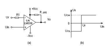
Figure 1 (b is its transmission characteristics)
Figure 2 below shows the overheat detection and protection circuit in an instrument. It is powered by a single power supply, and a fixed reference voltage is added to the inverting input of 1/4LM339, and its value depends on R1 and R2. UR=R2/(R1+R2)*UCC. The voltage at the non-inverting terminal is equal to the voltage drop of the thermal element Rt. When the temperature inside the machine is below the set value, the "+" terminal voltage is greater than the "-" terminal voltage, and Uo is at high potential. When the temperature rises above the set value, the "-" terminal voltage is greater than the "+" terminal, the comparator reverses, and the Uo output is zero potential, causing the protection circuit to operate. Adjusting the value of R1 can change the threshold voltage, which sets the temperature The size of the value.

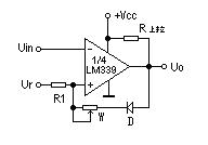
Figure 2 Hysteresis comparator

It is not difficult to see that once the output state is converted, as long as the interference near the jump voltage value does not exceed the value of ΔU, the value of the output voltage will be stable. But what comes with it is a reduction in resolution. Because for the hysteresis comparator, it cannot distinguish two input voltage values whose difference is less than ΔU. Adding positive feedback to the hysteresis comparator can speed up the response speed of the comparator, which is one of its advantages. In addition, since the positive feedback added by the hysteresis comparator is very strong, which is much stronger than the parasitic coupling in the circuit, the hysteresis comparator can also avoid self-oscillation caused by the parasitic coupling in the circuit.

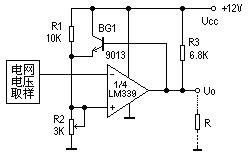
image 3
Figure 3 shows the grid overvoltage detection circuit part of an induction cooker circuit. When the grid voltage is normal, U4 of 1/4LM339 is <2.8V, U5=2.8V, the output is open circuit, the overvoltage protection circuit does not work, and the emitter follower BG1 as a positive feedback is turned on. When the grid voltage is greater than 242V, U4>2.8V, the comparator flips, the output is 0V, BG1 is cut off, and the voltage of U5 is completely determined by the voltage division value of R1 and R2, which is 2.7V, making U4 larger than U5, which means The state after flipping is extremely stable, and instability caused by small fluctuations in the grid voltage near the overvoltage point is avoided.
Due to the creation of a certain hysteresis (hysteresis), after overvoltage protection, when the grid voltage drops to 242-5=237V, U4<U3, the induction cooker starts to work again, which is exactly what we expect.

Double limit comparator (window comparator)
R1<Uin<UR2), the output is high potential (UO=UOH). When Uin is not within the threshold potential range, (Uin>UR2 or Uin<UR1) the output is low (UO=UOL), and the window voltage ΔU=UR2-UR1. It can be used to determine whether the input signal potential is between specified threshold potentials.

- Mobile phone interference circuit sharing
- How to use Tesseract for optical character recognition on Raspberry Pi
- Build a Raspberry Pi-based QR code scanner
- How to create a digital watch using YAKINDU Statechart Tools
- Designing a Simple Solar Voltage Regulator PCB
- Analysis of the circuit principle of ZX5-630 welding machine
- DIY Solar Detector
- How to create image processing solutions using HLS capabilities
- How to Design a Wireless Remote Controlled Two-Wheeled Robotic Rover Using ESP8266 and Arduino Uno
- Driving Large TFT-LCD Displays with Space-Saving Triple-Output Regulator
- How to learn circuit diagrams?
- Cycle timer circuit diagram with start and stop preset functions
- Inspection circuit diagram for broken rotor bar of three-phase motor
- Motorcycle ignition circuit diagram
- Typical super regenerative radio receiver circuit diagram
- Circuit diagram of wireless ECG monitoring system based on GPRS
- Konka lc-tm2008 LCD color TV video decoding circuit diagram
- Hitachi RAS-5102 inverter air conditioner remote control transmitter circuit diagram
- Electric iron automatic temperature adjustment principle circuit diagram
- Triangular wave oscillator using 2 operators


 京公网安备 11010802033920号