How does sand become chips?
Source: InternetPublisher:小胖友 Keywords: Chip transistor Updated: 2025/01/21
This article mainly explains the process of chip formation. How does sand become a chip? Before starting to introduce a series of basic concepts of electricity and various cumbersome formulas, I want to solve the doubts that most of us have always had. However, this question is still difficult to answer in a few sentences, and we need at least a dozen sections to complete all the knowledge contained here. Therefore, in this section, I will focus on answering the most interesting and important part: How does sand become a transistor?
1. From sand to chips - chip formation process
PN junction is a structure widely found in semiconductor devices. It is not actually a very accurate structure. PN junction is actually a phenomenon that refers to the depletion that occurs near the contact part of P-type semiconductor and N-type semiconductor.
There are a lot of terms here, and if I pull a little from various encyclopedias here and there, the combination is pretty much like this. At the beginning, the questions of why a diode has unidirectional conductivity, why a transistor can amplify current, and why a JFET can limit current bothered me one after another.
The problem with the textbooks of various universities is that they never explain the detailed principles, and even if they do, I still can't understand them, which leads to more and more problems, and it is difficult to remember the formulas and theories. It was not until recently that I finally understood their principles. In order to facilitate everyone to understand the following series of theories, the first part will be very detailed to lay a solid foundation for subsequent learning.
2. What is a semiconductor?
Let's talk about what semiconductors are. Semiconductors are materials that have conductive properties between those of conductors and insulators. We know that the difference between conductors and insulators is that there are a large number of free electrons in conductors, while there are almost no free electrons in insulators. So, can pure silicon crystals conduct electricity?
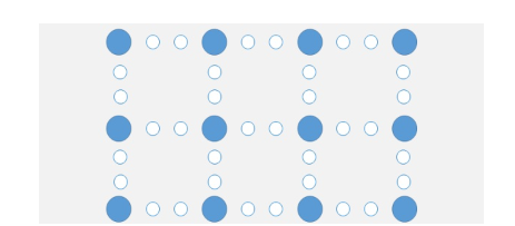
Pure silicon crystal
In the above picture, the blue solid spheres are silicon atoms, and the blue hollow spheres are electrons. Silicon atoms are tetravalent, so there are four electrons around one atom (8-4=4). Each silicon atom shares four electrons with the surrounding silicon atoms, forming a stable structure of eight electrons. In this case, there are almost no free electrons in the pure silicon crystal.
- The electrons are strongly bound by covalent bonds, so pure silicon crystals are insulators.
So how do we improve the conductivity of silicon crystals? The first method is to add free electrons. After adding free electrons, since electrons are negatively charged, we call the silicon crystal with free electrons an N-type semiconductor, where "N" is the abbreviation of "negative". The operation of adding free electrons is professionally called doping. Smart students can start with this term and think about how free electrons are added to the crystal.
We need to replace the silicon atom with an atom that has a higher valence than silicon, so that this atom will have 9 electrons around it. This extra electron will become a free electron and enhance the conductivity of the crystal. Doping This step is usually done by bombarding the silicon crystal in a vacuum using an ion beam. The ions will hit a portion of the silicon atoms and implant the desired atoms into the ion beam.
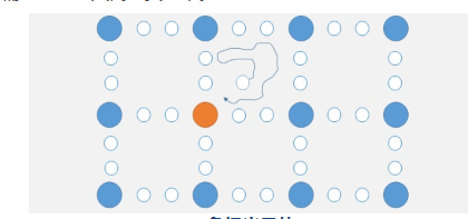
Negative semiconductor
What atoms have a higher valence than silicon? Phosphorus is an impurity with a very low content, which can be approximated as part of the crystal. Under normal circumstances, the extra electrons of phosphorus stay near the donor atom. However, once we apply voltage on both sides of the semiconductor material, since eight electrons are more stable than nine electrons, both Si and P atoms "drop" electrons, and it will become a free electron from the negative electrode of the battery. Run to the positive electrode of the battery. The free electrons moving in a directed manner generate electrical energy.

Directed motion of free electrons
Since we know that "N" stands for "negative", it follows naturally that "P" stands for "positive". Before explaining what a P-type semiconductor is, I must ask a few questions:
(1) How to reduce the number of electrons in silicon crystals?
(2) Should the impurities we use be more reactive or more stable?
(3) Are the properties of impurities closer to or further away from silicon?
(4) What kind of impurities are more likely to be added?
The answer is the fifth element, boron. Boron has several excellent properties. First, it is a major element of the third group, so its outermost layer has three electrons, one less than silicon, so when doping silicon crystals, there is an overall lack of free electrons. Second, boron is the only non-metallic element in the third group that is similar to silicon, and it has a strong similarity to silicon. Finally, boron is stable, lightweight, and easy to implant into silicon crystals.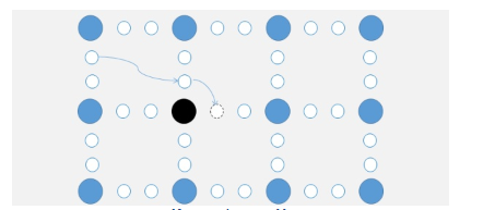
Injecting Boron into Silicon Crystals
Boron is a black powder solid, so I've replaced it here with a black ball. There's a dotted ball next to it. This is an electron hole, which means there's an electron missing at this location. So we can think of this hole as being positively charged.
We call electrons and holes charge carriers. They carry their own charge and can act as current generators. The concept of a hole may be too abstract, but we can understand it like this: imagine a hole as an air bubble in a glass of water. The gravitational potential of the glass is very low, so we imagine it as the negative terminal of a battery, and the bottom of the glass is the positive terminal.
Then we imagine the water molecules as electrons. The water molecules above the bubble will enter the bottom of the cup, and then a new bubble will be created at the location of the original water molecule, thus creating the illusion that the bubble is moving upward. In the circuit, the electron is also affected by the voltage to fill the hole. Then the position of the original electron is replaced by the hole. It seems that the hole moves from the positive electrode to the negative electrode.
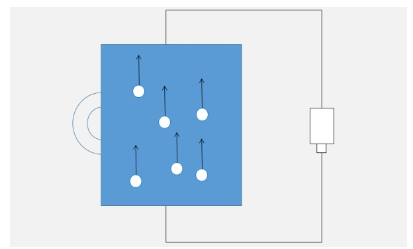
Charge carrier
III. PN Junction and Diode
Now we can finally talk about the PN junction. As we said before, the PN junction is a phenomenon that exists between a P-type semiconductor and an N-type semiconductor.

PN Junction
From now on, the color of P-type semiconductors will be represented by void orange, and the color of N-type semiconductors will be represented by electron blue.
Near the contact surface of the P-type semiconductor and the N-type semiconductor, the electrons of the N-type semiconductor are filled into the holes of the P-type semiconductor, resulting in no carriers in the PN junction. The attraction of the holes to the electrons is still very strong. In the part of the P-type semiconductor, the holes are filled with electrons, but the impurity contained in the P-type semiconductor is boron, and there are only three electrons outside the boron.
When the holes are filled, there are four electrons around the boron, one more electron, so the whole thing is negatively charged. Similarly, in the N-type semiconductor part, the electrons run into the holes of the P-type semiconductor, and there is one less electron around the phosphor, so the whole thing is positively charged. In this area, electrons fill all the holes [1], resulting in no free-moving carriers to carry charge, so current cannot pass through this area well. P-type semiconductors and N-type semiconductors can conduct electricity when they exist alone, but when they are put together, they have unidirectional conductivity, and at this time they form a diode.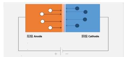
diode
We call the P-shaped semiconductor part of the diode the anode and the N-shaped semiconductor part the cathode. This is easy to understand. Recall the previous knowledge: the air current flows from the positive electrode to the negative electrode, and the electrons flow from the negative electrode to the positive electrode. The air current of the P-shaped semiconductor and the electrons of the N-shaped semiconductor squeeze toward the PN junction with the help of the forward voltage, so that the carriers on both sides of the PN junction regain and have the ability to conduct electricity. For silicon diodes, as long as the forward voltage exceeds 0.7V, the width of the PN junction will shrink to be short enough to allow current to pass through the diode.
I have replaced the above circuit symbol for the battery. Correspondingly, the diode also has its own circuit symbol, which is longer:
Diode circuit symbol
So what if we apply reverse voltage to the diode? You can think about the direction of movement of electrons and holes. Think about whether the width of the PN junction will change. What effect will this change have on the current?
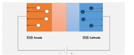
Apply reverse voltage to the diode
Similarly, holes will flow to the negative electrode, electrons will flow to the positive electrode, carriers will move away from the PN junction, and the area without carriers will become larger, so the PN junction will become wider, resulting in no current flow and a reverse voltage being applied. The larger the current, the smaller the current passing through the diode. Therefore, the diode has unidirectional conductivity and can only allow current to flow from the anode to the cathode. [2]
Current-Voltage Diagram
The graph above is a current-voltage graph that shows the current that can pass through a diode at different voltages. The red line in the graph represents a silicon diode and the blue line represents a germanium diode. Niobium, like silicon, is a very good semiconductor material. A diode has a value called the threshold voltage. Above this value, the diode starts to conduct. For a silicon diode, this value is 0.7V. For a germanium diode, this value is
0.2V[3]. There is also a value called breakdown voltage. We will mention this value when we talk about rectification.
With all this preparation done, we can finally talk about transistors. There are billions of transistors in the CPU, but these billions of transistors have exactly the same structure, only the connections have changed. The transistors used in the CPU can have their own name: MOSFET.
IV. Metal Oxide Semiconductor Field Effect Transistor
In 1926, when the Northern Expedition initiated by the Guangdong Nationalist Government was in full swing, on the other side of the ocean in the United States, physicist Julius Edgar Lilienfeld
Lilienfeld applied for a patent that had a significant impact on the development of electronics in the next century.
The patent first proposed the working principle of field effect transistors, which is a method and device for controlling current. From then until 1960, although two generations of field effect semiconductor devices, JFET and MOSFET, came out one after another, China did not make any contribution to them. To this day, China's semiconductor industry still lags behind the world level.
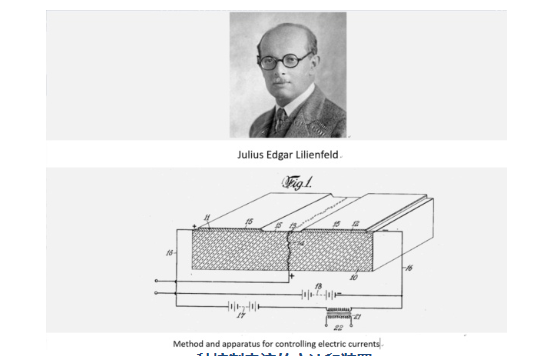
A method and device for controlling current
The full name of MOSFET is scary. Its English name is called Metal Oxide Semiconductor Field Effect Transistor. Its Chinese name is Metal Oxide Semiconductor Field Effect Transistor. I hope you can also appreciate the charm of MOSFET
- Negligibly low power consumption, extremely simple structure and processing technology, and fascinating working principle.
We noticed that the MOSFET is a field effect transistor. What is the field effect? We all learned about magnetic fields early on, and we know that opposites attract opposites. For electronics, electric fields are also generated. Just like electric and magnetic fields, it is likes repel and opposites attract. Electrons repel electrons, but electrons attract holes and vice versa. This sentence is simple, just to give students a concept. In the following sections, I will explain the electric field in detail.

electric field
We all know that the function of a transistor is to control a large current with a small current. So a transistor generally has three pins. Two are responsible for current input and output, and one is responsible for controlling on and off. The key is how to turn it on and off. We must make the input impedance as large as possible.
What is input impedance? Input impedance is the resistance value from the control pin to the output pin. If the input impedance is low, the current on the control pin will easily flow out of the output pin. Each control will be turned on and off a little bit. The current flows out of the output pin, which is a waste. If the input impedance is large, the current on the control pin will not easily flow out of the output pin because the resistor plays the role of blocking the current. The ideal state is that the input impedance is infinite, so that the control current does not consume energy at all, and the power consumption of the CPU can be reduced to almost zero.
MOSFET uses a very magical way to control the current. Its input pin and output pin are connected by two independent N-shaped semiconductors. The two N-shaped semiconductors are filled with P-shaped semiconductors. Above the middle P-shaped semiconductor, there is a thin layer of silicon dioxide (oxide) insulating layer, and above it is a metal plate, which connects the control pin.
So it's called a metal/oxide/semiconductor/field-effect/transistor.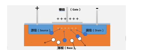
Field effect tube structure
In a MOSFET, we call the input pin the source G, the output pin the drain D, the control pin the gate G, and the large P-shaped semiconductor at the bottom the substrate B [4]. When there is no voltage on the gate, we can see that there are two PN junctions between the source-substrate-drain stages. These two PN junctions isolate the source and drain stages from which current flows. There is no direction in which current can flow.

N+ semiconductor channel
However, if we apply a positive voltage like the gate, then the positive charge on the gate metal plate will attract the negatively charged electrons of the P-type semiconductor and N-type semiconductor. Then, the area near the insulating layer is filled with carriers (electrons). As we all know, semiconductor materials containing electrons are N-type semiconductors. Although the substrate is essentially a P-type semiconductor, since the substrate has a very high electron concentration, we can treat the P-type semiconductor in this area as an N-type semiconductor containing free electrons. We call this area the channel. Since the semiconductor between the source and drain stages now has the same properties and both are N-type semiconductors, current can flow freely between the two pins.
5. N+ type semiconductor
In fact, the semiconductor used for the source and drain stages here is not an ordinary N-type semiconductor. Here, a large amount of N doped with phosphor is used.
+ semiconductors. They contain a large number of free electrons, which enables more electrons to be gated. The poles attract, increasing the width of the channel, making it easier for current to pass through. We can find that the gate and drain are insulated, which means that its input resistance is very high. It can be said that if it were not for the invention of MOSFET, the electricity generated in the world would not be able to afford a few computers. The emergence of MOSFET has enabled millions of transistor processors to enter millions of homes. Its simple structure also allows ordinary people to have powerful computing power.
Just as our world is made up of atoms, the electronic world is also made up of MOSFETs. No matter how complex something is, its essence is simple and beautiful. I hope this section can inspire students and inspire everyone to continue exploring the charm of electronic circuits.
- Which TVS diodes are suitable for RS232/RS485 and Controller Area Network applications?
- Ideal characteristics of operational amplifiers/pin configurations/gain types/primary applications
- What are the main types of resistors? Detailed explanation of the functions and uses of resistors
- Types and structures/characteristics/functions/implementations of smart sensors
- Analysis of the working principle of CMOS/CCD image sensor
- Introduction of TDA4863J/4863AJ TV field scanning IC
- Circuit diagram of a differential amplifier circuit
- Circuit diagram of an example of differential and integral circuits
- Homemade air conditioner outdoor unit shutdown indicator
- Sine wave divider (μA747, μA795)
- Transistor inverter circuit commonly used in radio medium wave band
- water saving circuit
- Touch switch power circuit
- Transistor controlled rectifier circuit a
- Transistor meter circuit c
- Transistor measuring instrument circuit b
- A single-section transistor performance test circuit
- Transistor leakage release protection circuit
- Two types of multi-stage negative feedback amplifiers b
- Transistor type AC arc welding machine no-load automatic stop circuit 2


 京公网安备 11010802033920号