Home >
Power Circuits >Switching DC to DC (DC-DC) > Discrete Design of Low-Cost Isolated 3.3V to 5V DC/DC Converter
Discrete Design of Low-Cost Isolated 3.3V to 5V DC/DC Converter
Source: InternetPublisher:失踪的猫 Keywords: DC/DC Updated: 2023/11/17
Isolated 3.3V to 5V converters are usually used in long-distance data transmission networks. In this network, the bus node controller operates from a 3.3V power supply to save power, and the bus voltage is 5V to ensure long-distance transmission. signal integrity and provide high drive capability. Although isolated DC/DC converter components for 3.3V to 5V conversion are already available on the market, integrated 3.3V to 5V converters are still difficult to find. Even when found, these specific converters (especially those with stable outputs) typically have long product lead times, are relatively expensive, and generally have certain isolation voltage limitations.
If the application requires isolation voltages above 2 kV, converter efficiencies above 60%, or the reliable availability of standard components, discrete designs are a low-cost alternative to integrated components. The disadvantage of discrete DC/DC converter design is that it requires a lot of work - choosing a stable oscillator structure and break-before-make circuitry, selecting MOSFETs that can be driven efficiently by standard logic gates, and conducting suitable temperature and long-term reliability testing. All of these efforts cost time and money. Therefore, before rushing into such a plan, designers should consider the following: Integrated components typically have passed temperature testing and have other industrial qualifications. Not only are these components the most reliable solutions, they also offer fast time to market.
Unstable output converters typically start at $4.50 to $5.00 per 1,000-piece unit, while stable output converters are typically twice that price, around $10.00 or more. Therefore, it makes sense to purchase a converter with an unstable output and either buffer the output with a buck capacitor or feed it into a low-cost, low-dropout regulator (LDO) such as TI's TPS76650.
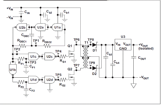
The discrete DC/DC converter design shown in Figure 1 uses only a few existing standard components (such as logic ICs and MOSFETs, etc.) to serve the transformer driver, and an LDO to stabilize the output voltage. The circuit was prototyped using many through-hole components, making it larger than integrated components, but board space was greatly reduced thanks to the use of TI's Little Logic? devices.
The main benefits of this design are a smaller bill of materials (BOM) and freedom in selecting the isolation transformer for isolation voltages ranging from 1 to 6kV. Our goal is to provide a low-cost alternative to fully integrated DC/DC converters and stand-alone transformer drivers for stable output by making the transformer driver stage.
Figure 1 Isolated 3.3V to 5V push-pull converter
operating principle
Low-cost, isolated DC/DC converters are generally push-pull driver types. The working principle is very simple. A square-wave oscillator with a push-pull output stage drives a center-tapped transformer, the output of which is rectified and can be used in stabilized or unsteady DC form. An important functional requirement is that the square wave must have a 50% duty cycle to ensure symmetrical magnetization of the transformer core. Another requirement is that the product of magnetizing voltage (E) and magnetizing time (T) (called the ET product in Vμs) must not exceed the transformer's typical ET product specified by its manufacturer. We must also install a break-before-make circuit close to the oscillator to prevent the two transformer legs of the push-pull output stage from conducting electricity at the same time and causing circuit failure. The well-known three-inversion gate oscillator of
discrete design
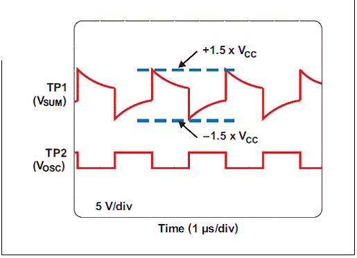
consists of U1a, U2a and U2b, which was chosen because it is relatively stable in terms of power supply fluctuations. Its normal frequency is set to 330kHz via a 100-pF ceramic capacitor (COSC ) and two 10-kΩ resistors (ROSC1 and ROSC2 ) . The oscillator has a duty cycle close to 50% and a maximum frequency fluctuation of less than ±1.5% over a supply voltage fluctuation range of 3.0-V to 3.6-V. Figure 2 shows the waveform at the summing point of R OSC1 and R OSC2 (TP1) and the oscillator output (TP2). All voltages are measured with respect to the reference circuit base voltage.
Figure 2 Oscillator waveforms of TP1 and TP2
If the application requires isolation voltages above 2 kV, converter efficiencies above 60%, or the reliable availability of standard components, discrete designs are a low-cost alternative to integrated components. The disadvantage of discrete DC/DC converter design is that it requires a lot of work - choosing a stable oscillator structure and break-before-make circuitry, selecting MOSFETs that can be driven efficiently by standard logic gates, and conducting suitable temperature and long-term reliability testing. All of these efforts cost time and money. Therefore, before rushing into such a plan, designers should consider the following: Integrated components typically have passed temperature testing and have other industrial qualifications. Not only are these components the most reliable solutions, they also offer fast time to market.
Unstable output converters typically start at $4.50 to $5.00 per 1,000-piece unit, while stable output converters are typically twice that price, around $10.00 or more. Therefore, it makes sense to purchase a converter with an unstable output and either buffer the output with a buck capacitor or feed it into a low-cost, low-dropout regulator (LDO) such as TI's TPS76650.
The discrete DC/DC converter design shown in Figure 1 uses only a few existing standard components (such as logic ICs and MOSFETs, etc.) to serve the transformer driver, and an LDO to stabilize the output voltage. The circuit was prototyped using many through-hole components, making it larger than integrated components, but board space was greatly reduced thanks to the use of TI's Little Logic? devices.
The main benefits of this design are a smaller bill of materials (BOM) and freedom in selecting the isolation transformer for isolation voltages ranging from 1 to 6kV. Our goal is to provide a low-cost alternative to fully integrated DC/DC converters and stand-alone transformer drivers for stable output by making the transformer driver stage.
Figure 1 Isolated 3.3V to 5V push-pull converter

operating principle
Low-cost, isolated DC/DC converters are generally push-pull driver types. The working principle is very simple. A square-wave oscillator with a push-pull output stage drives a center-tapped transformer, the output of which is rectified and can be used in stabilized or unsteady DC form. An important functional requirement is that the square wave must have a 50% duty cycle to ensure symmetrical magnetization of the transformer core. Another requirement is that the product of magnetizing voltage (E) and magnetizing time (T) (called the ET product in Vμs) must not exceed the transformer's typical ET product specified by its manufacturer. We must also install a break-before-make circuit close to the oscillator to prevent the two transformer legs of the push-pull output stage from conducting electricity at the same time and causing circuit failure. The well-known three-inversion gate oscillator of
discrete design
consists of U1a, U2a and U2b, which was chosen because it is relatively stable in terms of power supply fluctuations. Its normal frequency is set to 330kHz via a 100-pF ceramic capacitor (COSC ) and two 10-kΩ resistors (ROSC1 and ROSC2 ) . The oscillator has a duty cycle close to 50% and a maximum frequency fluctuation of less than ±1.5% over a supply voltage fluctuation range of 3.0-V to 3.6-V. Figure 2 shows the waveform at the summing point of R OSC1 and R OSC2 (TP1) and the oscillator output (TP2). All voltages are measured with respect to the reference circuit base voltage.
Figure 2 Oscillator waveforms of TP1 and TP2
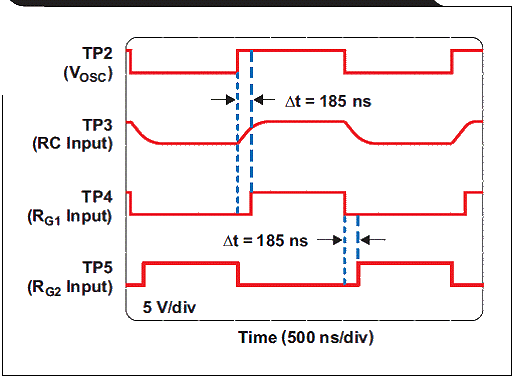
The NAND gates (U1c, U1d) of the Schmitt trigger circuit implement the first-off-then-on function to avoid overlapping of MOSFET conduction phases. The other two NAND gates (U2c, U2d) are configured as inverting buffers to generate the correct signal polarity necessary to drive the N-channel MOSFETs (Q1, Q2). Figure 3 shows the complete break-before-make action. To accommodate the limited drive capabilities of standard logic gates, MOSFETs were chosen because of their lower total charge and shorter response time.
Figure 3 Break-before-make waveform
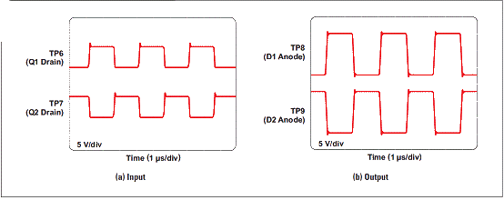
The isolation transformer (T1) has a 2:1 secondary to primary turns ratio, a 0.9 mH primary coil inductance, and a guaranteed isolation voltage of 3kV. Figure 4 shows the input and output waveforms of the transformer.
Figure 4 Transformer Waveforms
Both diodes (D1, D2) are fast Schottky rectifiers that provide low forward voltage while performing full-wave rectification at full load current (VFW < 0.4 V at 200 mA). It is possible to obtain the output voltage directly from the step-down capacitor (Cb3) behind these diodes. In this case, the output is unstable but has the maximum efficiency of the DC/DC converter. However, designers must ensure that the maximum supply voltage of the affected circuit is not exceeded, which is more likely to occur at low load or open circuit conditions. If the unregulated output voltage at minimum load conditions is too high, a linear regulator must be used after the full-wave rectifier to provide a stable output supply voltage.
The main benefit of linear regulators is low ripple output. Other benefits include short-circuit protection and over-temperature shutdown. However, the main disadvantage is that it is very inefficient.
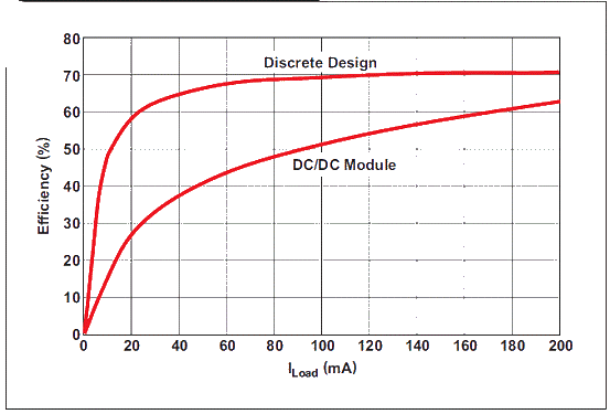
Figure 5 shows the ripple of the circuit shown in Figure 1 at an output voltage of 4.93 V, while Figure 6 compares the efficiency of this circuit to an integrated DC/DC component with a stable output.
Figure 5 Output ripple when V OUT
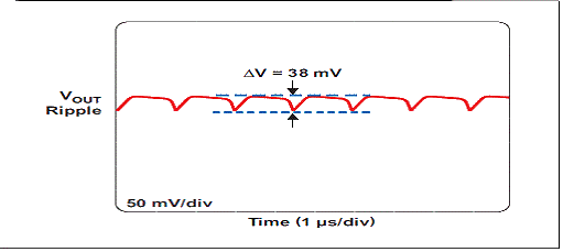
=4.93V Figure 6 Efficiency comparison
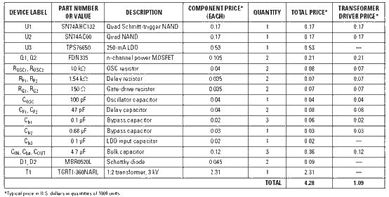
The following table provides the BOM of the discrete DCDC converter. Note that the bypass capacitor value is larger than the 10 nF commonly used in some low-speed applications. This is because high-speed CMOS technologies (eg AHC, AC, LVC, etc.) have highly dynamic loads, so the bypass capacitor value must be 0.1 μF or higher to ensure proper operation. This is particularly important for the inverting buffer driving the MOSFET, which has a bypass capacitor value of 0.68 μF.
Conclusion
Without board space constraints, discrete designs of isolated 3.3-V to 5-V DC/DC converters with stable outputs can be a realistic, low-cost alternative to stable-output integrated DC/DC components. The main benefit of a discrete design is the freedom to select the isolation transformer to meet various isolation voltage requirements.
Latest Power Circuits Circuits
- Analysis of the working principle of switching regulator
- Basic characteristics of power field effect tubes, how to improve the dynamic performance of power MOSFET
- How about the boost converter TPS61299?
- A very convenient small power supply circuit to share
- Fabrication of multi-cell lithium battery charging circuit
- Energy-saving motorcycle rectifier regulator
- ISO113 circuit that can reduce power consumption
- LED Driver ZD1680
- Miniature polarity reversal power supply using MAX1721
- Dual forward converter schematic diagram
Popular Circuits
- LTC3525: Compact, High-Efficiency Boost Converter for Single-Cell Alkaline Batteries
- Switching power supply circuit composition and detailed explanation of each part (1)
- Power circuit with smoothing filter capacitor
- 4-phase CPU power circuit using HIP6301 and HIP6602 chips
- Transistor stabilized current power supply circuit 2
- One of the transistor stabilized current power supply circuits
- Household emergency power circuit 02
- Head amplifier dedicated power supply circuit
- Common power circuits and applications 05
- Common power circuits and applications 01


 京公网安备 11010802033920号