With the development of electronic technology and network technology, the use of power lines as carriers for signal transmission has received more and more attention and has been widely used. Power lines are the most common and widely covered physical media today, and the power grid formed by them is a nearly natural physical network. How to utilize the resource potential of the power grid and combine the power transmission network and the communication network without affecting the transmission of electric energy, so that it can become another communication network after telecommunications, telephones, wireless communications, and satellite communications, has been a hot topic for technical research by domestic and foreign scientific and technological personnel for many years. Power line carrier communication was born in this context. It uses the power grid as a channel to realize data transmission and information exchange. As the transmission medium of carrier signals, power lines are the only wired communication method that does not require line investment.
As an emerging application field of communication technology, power line carrier communication technology has attracted worldwide attention for its attractive prospects and potential huge market. China has been engaged in the research of power line carrier communication technology since the 1950s. After the 1990s, the demand for power line carrier technology has further expanded with the development of China's economy. At present, this technology has begun to be applied to home automation, remote meter reading, broadband Internet access and other fields. Experts say that in some industrial fields with large interference and difficult wiring, the use of power line carrier communication can achieve twice the result with half the effort to achieve automatic control. Therefore, the power grid is also known as the "untapped gold mine".
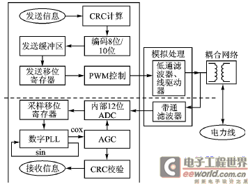
There are many ways to implement power line carrier communication. Usually, a dedicated communication chip is used to implement the modulation and demodulation part of the system, while the application part of the system is completed by another controller. This two-chip method is a good choice. With the development of digital signal processing technology, the two can be combined into one. An advanced DSP controller can realize the function of a power line modem. The DSP controller can implement the modem function in software and use on-chip peripherals to realize reception and transmission on the power line through the analog terminal interface. This article describes a system that complies with the CEA709[1] protocol and uses a fixed-point DSP controller (TMS320LF2812) to implement a power line modem from software and hardware. The article describes the specific design method of the analog terminal, which is necessary for the stable transmission and reception process. 1 System framework based on the CEA709 protocol Figure 1 is a physical block diagram of the ANSI/CEA709 protocol standard. A detailed description of the protocol can be found in reference [1].
|
|
Figure 1 CEA709 protocol physical layer block diagram |
LonWorks, a widely used control network platform in rail transit, network energy management, intelligent buildings, HVAC, coal mine safety, energy and environmental management, has become a guiding technical document for China's national standards. The global building, home, industrial and transportation automation industries currently use a large number of LonWorks-based platforms. The LonWorks platform is the core technology platform of the world's largest residential smart meter network, and is used by smart meters for residential and small commercial meters in countries such as Sweden, the Netherlands and Australia. The protocol running on this platform is the US control network standard ANSI/CEA709. At present, more and more Chinese manufacturers and integrators have adopted the ANSI/CEA709 protocol standard. For example, on the Qinghai-Tibet Railway, the world's longest high-altitude railway train, the LonWorks technology platform is used to use the ANSI/CEA709 protocol for technical monitoring and control of various systems, including monitoring of the most advanced passenger oxygen supply system.
For the CEA709 physical layer block diagram in Figure 1, the system block diagram using DSP to implement the CEA709 modem function is shown in Figure 2. The DSP (TMS320F2812) has a computing power of 150 MIPS. Signal acquisition uses a 12-bit on-chip analog/digital converter with a conversion speed of 12 Msps. The DSP provides multiple PWMs to accommodate power line modems.
|
|
|
Figure 2 System Block Diagram |
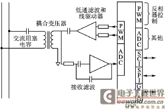
Two on-chip PWM outputs and one line driver are used to implement the modem's transmit function. An A/D input is used to sample the bandpass input port signal to implement the modem's receive function. The bandpass filter is actually a discrete filter. Together with the AC blocking capacitor and coupling transformer, they complete the analog front-end design of the interface.
The following mainly introduces the design process of the analog front-end interface.
2 Implementation of analog front end and interface
The CEA709 communication system is defined by a 131.579 kHz carrier frequency. Each transmitted data bit consists of 24 cycles of the carrier frequency sine wave, so the baud rate is 5.5 kbps. The phase of each bit segment can be set to 0° to make the position 0, or set to 180° to make the position 1.
2.1 Signal reception
First, the 50/60 Hz power line voltage in the coupling network is removed, and then a second-order active bandpass filter is used to filter out the signal. The 131.5 kHz frequency modulation signal can be detected. This filter is established by an operational amplifier. The output of the bandpass filter is sampled by a channel of the DSP's analog/digital converter, and the signal sampling sequence is processed by a FIR filter. At the same time, the output of this filter is used for clock recovery and data detection.
The sampled received signal is 115 kHz, which is (21/24) times the carrier frequency. This signal is downsampled in the range of 131.5 kHz to an intermediate frequency of 16.5 kHz, and then mixed and multiplied with the input carrier sinusoidal signal using the sampling frequency clock. The result of multiplying the two sinusoidal waves generates a composite signal of the "sum" and "difference" of the two sinusoidal wave frequencies, as shown in Figure 3.

|
|
Figure 3 Frequency effect after sampling |
During operation, the DSP generates an interrupt after each ADC sample conversion is completed, and then each sample signal is compared with the digital PLL (PhaseLocked Loop) output to estimate the phase of the received signal. At a frequency of 5.5 kHz, the phase is determined. If the phase is less than ±90°, it is assumed that a "0" signal is received, otherwise it is a "1" signal. The
received bit sequence is compared with the known "bit synchronization" field. When the bit synchronization data is received, the modem starts searching for the "word synchronization" field. The word synchronization data marks the beginning of the message data and also defines the polarity of the message data. When the data of the packet is determined, the 11-bit codeword is decoded into an 8-bit data byte, the check bit of the received byte is compared with the calculated check bit, and the data is transmitted from the physical layer to the MAC layer. The received data is then compared with the CRC check, and the correct data is transmitted from the data link layer to the network layer.
2.2 Phase Detection
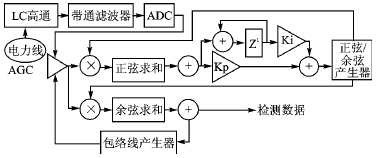
In order to detect the "0" or "1" of the transmitted signal, the phase of the intermediate frequency signal 16.5 kHz is in the form of discrete received signal values. First, a digital phase-locked loop (PLL) is driven by the received sampling signal. When the output of the PLL is synchronously locked to the received signal, the estimate of the complex phase between the PLL and the received signal is generated by the PLL modulation. The real part of the complex phase is the sum of cosines, which is a large positive value when a "0" signal is received; conversely, it is a large negative number when a "1" signal is received. The imaginary part of the complex phase is the sum of sines. It represents the phase deviation and is fed back to the PLL to adjust the sinusoidal output to track the received signal.
|
|
Figure 4 Receive signal processing block diagram |
Figure 4 is a complete block diagram of the received signal processing. In order to improve the stability of the system, an automatic gain control module (AGC) is added. It receives the signal by detecting the average size of the received signal.
2.3 Signal transmission
In this application, the transmit signal is directly generated by the on-chip PWM (pulse width modulation module) of the DSP controller. Each bit is defined as 24 cycles, so the PWM controller is allowed to run for 24 cycles; then, according to the polarity of the next transmit bit, an interrupt is used to reassign the PWM output. The message data to be sent is transmitted from the application layer to the session layer, transport layer, network layer, data link layer, and then to the physical layer to form a transmit waveform. At the data link layer, the CRC word of the message data is calculated and attached to the data. The physical layer determines whether the channel is available and then sends the data.
2.4 PWM generates the transmit waveform
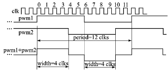
The three-level signal waveform is obtained by adding the two PWM outputs of the DSP controller, and then the waveform is generated as a sine wave by a low-pass filter. Compared with the standard two-level square wave, the odd harmonic energy of the three-level waveform is much smaller, and different pulse widths will produce different harmonic frequencies. In order to minimize the harmonics that the filter needs to remove, it is necessary to determine the optimal pulse width. This width can be found from the Fourier series formula for symmetrical pulses. In formula (1), T represents the fundamental frequency period and ω represents the pulse width.

|
Then, the total harmonic distortion THD can be expressed as follows:

|
|
|
|
Figure 5 Three-level waveform structure |
To minimize the total harmonic distortion of equation (2), the optimal pulse width is about 37% of the period T; however, this does not take into account the effect of low-pass filtering. If a second-order low-pass filter is used, different results will be obtained. In simulation, the Q of the second-order low-pass filter is set to 2.3. If the Q is large, THD will be better, but it will cause inter-symbol interference. Therefore, it is best to set the positive and negative digital pulse widths to 1/3 of the pulse period and set the low-pass filter angular frequency to the same as the frequency of the digital pulse sequence. The 1/3 pulse width can be obtained by using a timing clock signal that is 12 times the frequency of the transmitted waveform, as shown in Figure 5. By using an analog circuit to add the two digital signals and then filtering out the harmonics with a low-pass filter, a sine wave can be obtained from the PWM output.
|
|
|
Figure 6 Transmit low-pass filter amplifier |
2.5 Transmit Amplifier Design
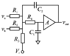
The transmit amplifier is determined by the SallenKey filter, and the transmit low-pass filter amplifier is shown in Figure 6. The transfer function of this circuit is as follows:

|
Here, R1=kR, R2=R, C1=C, C2=aC. Assuming the amplifier gain is 2, vout can be expressed as follows:

|
The peak of the filter is greatest when Q is greatest, and Q is greatest when the quotient k/(1+k) is 1.
Therefore, the resistors R1 and R2 in the SallenKey filter in Figure 6 are generally equal, and Q is determined by the ratio of the capacitors. The transmitting amplifier has two input terminals, and the two input signals are filtered from the signals in the PWM output terminal of the processor. The larger the peak value of the amplifier's transmitting frequency, the greater the relative attenuation in the harmonic frequency. Therefore, it is hoped that the parallel combination of resistors R1, R2, and R3 is equal to the resistance of R4 to obtain a larger Q value.
If R4=R is defined, then:
|
|
In addition, the attenuation factor k is defined as:

|
Then, the resistance value can be defined based on R and k:
|
|
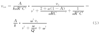
Define the capacitance as C1=C, C2=aC, according to A, k, a, R and C, the transmission function of the transmitting amplifier is as follows:
|
in:
|
|
Given Q, the capacitance ratio is:
|
|
If the amplifier gain A = 2, and the smaller solution of a is taken, then
|
|
Finally, s=0, the transfer function gain is:
|
|
In this way, all the parameters defining the transmission amplifier components are obtained, and the modem simulation terminal can be designed with the above parameters.
3 Conclusions
This paper only describes the hardware design process of the power line modem. The software design is mainly completed by DSP according to the requirements of the CEA709 protocol. There are still many key technical problems to be solved in the design and implementation, which are not described in detail due to space limitations. This modem hardware system based on a single fixed-point DSP control is tested under various power conditions. Its functions are relatively stable and reliable, and it is being used in smart home systems.
Previous article:Design of high-precision servo position loop based on TMS320F2812
Next article:A control system design based on DSP+FPGA
- Popular Resources
- Popular amplifiers
- Huawei's Strategic Department Director Gai Gang: The cumulative installed base of open source Euler operating system exceeds 10 million sets
- Analysis of the application of several common contact parts in high-voltage connectors of new energy vehicles
- Wiring harness durability test and contact voltage drop test method
- Sn-doped CuO nanostructure-based ethanol gas sensor for real-time drunk driving detection in vehicles
- Design considerations for automotive battery wiring harness
- Do you know all the various motors commonly used in automotive electronics?
- What are the functions of the Internet of Vehicles? What are the uses and benefits of the Internet of Vehicles?
- Power Inverter - A critical safety system for electric vehicles
- Analysis of the information security mechanism of AUTOSAR, the automotive embedded software framework
 Professor at Beihang University, dedicated to promoting microcontrollers and embedded systems for over 20 years.
- Innolux's intelligent steer-by-wire solution makes cars smarter and safer
- 8051 MCU - Parity Check
- How to efficiently balance the sensitivity of tactile sensing interfaces
- What should I do if the servo motor shakes? What causes the servo motor to shake quickly?
- 【Brushless Motor】Analysis of three-phase BLDC motor and sharing of two popular development boards
- Midea Industrial Technology's subsidiaries Clou Electronics and Hekang New Energy jointly appeared at the Munich Battery Energy Storage Exhibition and Solar Energy Exhibition
- Guoxin Sichen | Application of ferroelectric memory PB85RS2MC in power battery management, with a capacity of 2M
- Analysis of common faults of frequency converter
- In a head-on competition with Qualcomm, what kind of cockpit products has Intel come up with?
- Dalian Rongke's all-vanadium liquid flow battery energy storage equipment industrialization project has entered the sprint stage before production
- Allegro MicroSystems Introduces Advanced Magnetic and Inductive Position Sensing Solutions at Electronica 2024
- Car key in the left hand, liveness detection radar in the right hand, UWB is imperative for cars!
- After a decade of rapid development, domestic CIS has entered the market
- Aegis Dagger Battery + Thor EM-i Super Hybrid, Geely New Energy has thrown out two "king bombs"
- A brief discussion on functional safety - fault, error, and failure
- In the smart car 2.0 cycle, these core industry chains are facing major opportunities!
- The United States and Japan are developing new batteries. CATL faces challenges? How should China's new energy battery industry respond?
- Murata launches high-precision 6-axis inertial sensor for automobiles
- Ford patents pre-charge alarm to help save costs and respond to emergencies
- New real-time microcontroller system from Texas Instruments enables smarter processing in automotive and industrial applications
- [TI recommended course] #DC/DC switching regulator packaging innovation#
- ST60 short-distance, contactless connector evaluation 1: application environment and principle
- Looking for open source enthusiasts to improve the BabyOS open source project
- Can experienced friends recommend some useful power modules?
- What is the appropriate sampling rate for an oscilloscope?
- In what fields are panoramic high-definition video recorders used?
- What is the development trend of machine vision surface defect detection system?
- What does the MCU REFO pin stabilization time mean? How is it related to the connected capacitor?
- [Project source code] Static address alignment and dynamic address alignment of NIOS II custom IP core
- How to design a suitable power supply

 TLC2201ID


 京公网安备 11010802033920号