1 Introduction
The frequency source is the heart of modern RF and microwave electronic systems. Its performance directly affects the function of the entire electronic system and becomes a very important component.
Frequency sources are divided into two categories: self-excited oscillation sources and synthetic frequency sources. Common self-excited oscillation sources include crystal oscillators, cavity oscillators, dielectric oscillators, voltage-controlled oscillators, YIG oscillators, and waveform generators. The output frequency range, tuning bandwidth, and near-end phase noise of these frequency sources vary. The main advantages of synthetic frequency sources are high frequency stability, especially low phase noise, some of which are even lower than the phase noise of atomic clocks, flexible use, easy control, and superior performance. The disadvantages are high cost and high technical difficulty. In modern engineering design, the requirements for technical indicators such as frequency stability, accuracy, and frequency range of frequency sources are getting higher and higher. In many cases, frequency synthesis technology must be used to meet these requirements of modern electronic systems.
Frequency synthesis refers to the technology of generating a large number of discrete frequencies with the same stability and accuracy through a series of arithmetic operations on a standard signal frequency with high precision and high stability.
Phase-locked frequency source has the advantages of high frequency stability, pure spectrum, small parasitic clutter and low phase noise, and has been widely used in various communication and radar systems. The author designed a 1.8 GHz phase-locked frequency source using frequency division phase-locked frequency synthesis technology.
2 Principle of Phase-Locked Loop Technology
The methods for realizing frequency synthesis can be divided into direct synthesis and indirect synthesis. The characteristics of the two frequency synthesis technologies are shown in Table 1.

The phase-locked loop (PLL) is an automatic phase control system consisting of a phase detector (PD), a loop filter (LF) and a voltage-controlled oscillator (VCO), as shown in Figure 1.

The phase detector is a phase comparison device used to compare the phase of the reference signal Ur(t) and the voltage-controlled oscillator output signal Uo(t), and generate an error voltage Ue(t) corresponding to the phase difference between the two signals. The function of the loop filter is to filter out the high-frequency components and noise in the error signal Ue(t) to ensure the required performance of the loop and increase the stability of the system. The voltage-controlled oscillator is controlled by the output voltage Uo(t) of the loop filter, so that the oscillation frequency approaches the reference frequency, and the beat frequency of the two becomes lower and lower until the frequencies of the two are the same and a small residual phase difference is maintained. The following is a general description of the working process of the phase-locked loop:
The phase-locked loop (PLL) is a feedback control circuit like the AGC and AFC circuits. It is a phase error control system that compares the phase between the reference signal and the output signal, generates a phase error voltage to adjust the phase of the output signal to achieve the same frequency as the reference signal, thereby tracking the frequency drift of the signal. When the same frequency is achieved, the stable phase difference between the two signals can also be made very small.
The phase detector is a phase comparison device. It compares the phase of the input signal and the output signal Uo(t) of the voltage-controlled oscillator to generate an error voltage Ue(t) corresponding to the phase difference between the two signals. The function of the loop filter is to filter out the high-frequency components and noise in the error voltage, Ue(t) to ensure the performance required by the loop and increase the stability of the system. The voltage-controlled oscillator is controlled by the output voltage Uo(t) of the loop filter, so that the oscillation frequency approaches the reference frequency, and the beat frequency of the two is getting lower and lower, so that the two frequencies are the same and a small residual phase difference is maintained until the frequency difference is eliminated and locked. When the loop starts working, if the input signal frequency is different from the voltage-controlled oscillator frequency, the phase difference between the two signals will keep changing due to the inherent frequency difference between the two signals, and as a result, the error voltage output by the phase detector changes within a certain range. Under the control of this error voltage, the frequency of the voltage-controlled oscillator is also changing. Therefore, phase locking means that the voltage-controlled oscillator is controlled by an external reference signal so that the phase of the output signal of the voltage-controlled oscillator and the phase of the external reference signal maintain a certain specific relationship, so as to achieve the purpose of phase synchronization or phase locking. If the frequency of the voltage-controlled oscillator can be changed to be equal to the frequency of the input signal, it will stabilize at this frequency under the stability condition. After reaching stability, the frequency difference between the input signal and the output signal of the voltage-controlled oscillator is zero, the phase difference no longer changes with time, and the error voltage is a fixed value. At this time, the loop enters the "locked" state. This is the general process of the phase-locked loop.
The technical difficulty of phase-locked source design is how to reduce phase noise as much as possible. The following introduces the basic concept of phase noise and the causes of its generation, so that corresponding measures can be taken to reduce the phase noise of the frequency source.
3 Concept and Characterization of Phase Noise
Phase noise generally refers to the random fluctuations in the output signal phase caused by various noises in the system. The so-called short-term frequency stability refers to the phase fluctuations or frequency fluctuations caused by random noise. As for the slow frequency drift caused by temperature, aging, etc., it is called long-term frequency stability. Usually we mainly consider the problem of short-term frequency stability, which is generally expressed by phase noise.
An ideal sine wave signal can be expressed as follows:
In the formula, V(t) is the instantaneous amplitude of the signal, Ao is the nominal amplitude, and fo is the nominal frequency. At this time, the spectrum of the signal is a one-line spectrum. However, since any signal source has various noises, each noise component is different, making the actual output become:
When studying the measurement of phase noise, considering that the amplitude noise modulation power of the oscillator is much smaller than the phase noise modulation power, |ε(t)|<
The measurement of j(t) can be expressed by various types of spectral density. Obviously, the phase fluctuation is △j(t) and the frequency fluctuation is △f(t)=[dj(t)/dt]/2π. The commonly used relative frequency fluctuation function is:
Due to the existence of phase noise j(t), the frequency source is unstable. This instability is often characterized by the time domain Allan variance σ2y(2,t,t) and the frequency domain relative single sideband power spectrum (abbreviated as power spectrum) XXXX.
They are defined as:
Where: XXXXX is the frequency average value obtained from two consecutive measurements at the measurement sampling time XXX.
Where: PSSB(f) is the power spectral density of a phase noise modulation sideband at frequency f, and P0 is the carrier power. [page]
4 Phase noise analysis of each component of the system
The phase-locked loop frequency synthesizer is mainly composed of basic circuits such as frequency multiplier, amplifier, divider, mixer, phase detector, oscillator, etc. It also includes auxiliary capture circuit, frequency hopping control circuit and electronic switch, etc., which will introduce noise to the frequency synthesizer to varying degrees.
4.1 Oscillator
The noise of the oscillator is mainly determined by the loaded Q1 value of the resonant circuit, the noise of the resonant circuit and the noise of the oscillator device itself. The oscillator noise mainly consists of four parts:
(1) Phase noise generated by flicker noise frequency modulation.
(2) Phase noise caused by shot noise and thermal noise frequency modulation.
(3) Phase noise caused by flicker noise phase modulation.
(4) The phase noise generated by the phase modulation of shot noise and thermal noise is white noise.
There are two differences between VCO phase noise and crystal oscillator: first, the VCO resonant loop has a low Q value. The wider the VCO operating frequency band, the lower the Q value; second, there is a varactor diode in the VCO resonant loop, which has the same noise as the oscillator device. In addition, VCO phase noise is also proportional to the voltage-controlled tuning sensitivity.
Due to the low Q value of the resonant circuit, the near-end phase noise of the broadband tuned VCO is poor, 20 dB to 40 dB higher than that of the oscillator without a voltage-controlled reactance circuit. However, since the VCO output signal power is greater than that of the crystal oscillator, the far-end phase noise of the VCO is lower than the phase noise of the crystal oscillator after frequency multiplication.
4.2 External Noise
After N-fold frequency multiplication, the external noise will increase by 20lgNdB, and the internal noise converted to the device input will also increase by 20lgNdB. Therefore, when designing the frequency multiplier, attention should be paid to reducing its internal noise.
4.3 Frequency Divider
When the signal passes through the divider, the noise at the input end is usually reduced by 20logNdB. If the division factor is very high or the input signal phase noise is very low, the minimum noise is determined by the divider noise and the noise of the active circuit after the divider.
5. Specific design and implementation of phase-locked source
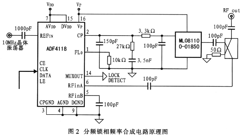
In the design of the frequency source, the frequency division phase detector uses ADF4118 from ADI of the United States; the voltage controlled oscillator VCO uses ML08l100-01850 from M/A-COM; the loop filter is composed of a third-order RC low-pass filter circuit, and its circuit principle is shown in Figure 2.

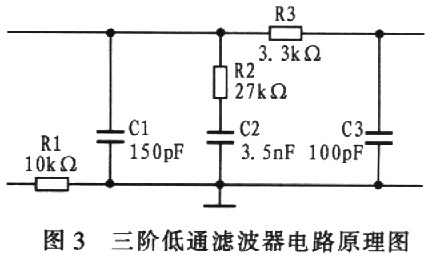
The key to the design of the phase-locked source is the design of the loop filter. The simplest and cheapest low-pass filter is the basic RC low-pass filter. This filter does not have a precise cutoff frequency, and the typical slope is 6 dB/lO octave, so the -3 dB point of the circuit should be designed to be close to the fundamental frequency of the current signal. A better solution is to use a third-order RC filter, the principle of which is shown in Figure 3.

When the passband of the loop filter of the phase-locked loop is narrow and the capture band is also narrow, the good tracking characteristics of the phase-locked loop can be used to achieve narrowband filtering of high-frequency input signals; filtering of tens of hertz or even several megahertz can be achieved at frequencies of tens of hertz, thereby filtering out noise and interference mixed in the input signal, which is difficult for other filters to do.
6 Test Data
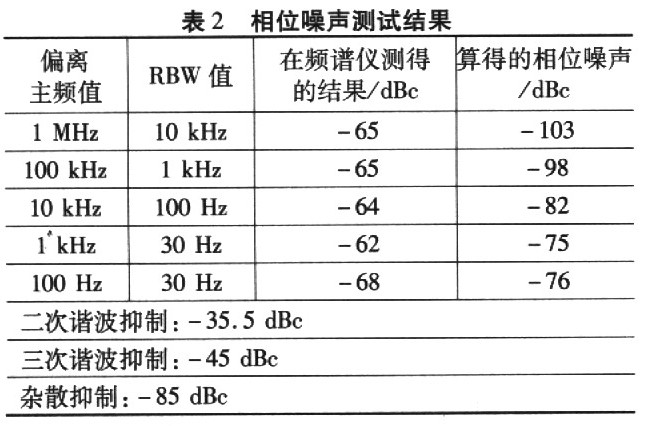
After the phase-locked source was successfully designed, the author tested it. The output frequency was 1 835 MHz, the output power was -4.2 dBm, and the phase noise test results are shown in Table 2.

From the data in Table 2, it can be seen that when the input frequency is 1 835 MHz, the output power is -4.2 dBm, the phase noise is -75 dBc/KHz, and the spurious suppression is -85 dBc, which fully meets the expected design technical indicators.
7 Conclusion
The frequency source is designed according to the requirements of the LO source for the RF subsystem of the mobile communication base station and the repeater. According to the experimental results, it can be seen that the phase-locked source obtained by using the ADI phase-locked loop (ADF4118) is 10 dB~20 dB better than the phase-locked source using the Freescale MCl45 series phase-locked loop introduced in the relevant data at the 1835 MHz frequency point, and the corresponding phase noise is 10 dB~20 dB better when used in the frequency shift module.
The success of this design further verifies that the phase-locked frequency source has the advantages of high frequency stability, pure spectrum, small parasitic interference and low phase noise. This method is simple in design, highly reliable and highly anti-interference.
Previous article:Ultrasonic object detection circuit design
Next article:Basic Principles of Resistor Current Sensing
- Keysight Technologies Helps Samsung Electronics Successfully Validate FiRa® 2.0 Safe Distance Measurement Test Case
- From probes to power supplies, Tektronix is leading the way in comprehensive innovation in power electronics testing
- Seizing the Opportunities in the Chinese Application Market: NI's Challenges and Answers
- Tektronix Launches Breakthrough Power Measurement Tools to Accelerate Innovation as Global Electrification Accelerates
- Not all oscilloscopes are created equal: Why ADCs and low noise floor matter
- Enable TekHSI high-speed interface function to accelerate the remote transmission of waveform data
- How to measure the quality of soft start thyristor
- How to use a multimeter to judge whether a soft starter is good or bad
- What are the advantages and disadvantages of non-contact temperature sensors?
- Innolux's intelligent steer-by-wire solution makes cars smarter and safer
- 8051 MCU - Parity Check
- How to efficiently balance the sensitivity of tactile sensing interfaces
- What should I do if the servo motor shakes? What causes the servo motor to shake quickly?
- 【Brushless Motor】Analysis of three-phase BLDC motor and sharing of two popular development boards
- Midea Industrial Technology's subsidiaries Clou Electronics and Hekang New Energy jointly appeared at the Munich Battery Energy Storage Exhibition and Solar Energy Exhibition
- Guoxin Sichen | Application of ferroelectric memory PB85RS2MC in power battery management, with a capacity of 2M
- Analysis of common faults of frequency converter
- In a head-on competition with Qualcomm, what kind of cockpit products has Intel come up with?
- Dalian Rongke's all-vanadium liquid flow battery energy storage equipment industrialization project has entered the sprint stage before production
- Allegro MicroSystems Introduces Advanced Magnetic and Inductive Position Sensing Solutions at Electronica 2024
- Car key in the left hand, liveness detection radar in the right hand, UWB is imperative for cars!
- After a decade of rapid development, domestic CIS has entered the market
- Aegis Dagger Battery + Thor EM-i Super Hybrid, Geely New Energy has thrown out two "king bombs"
- A brief discussion on functional safety - fault, error, and failure
- In the smart car 2.0 cycle, these core industry chains are facing major opportunities!
- The United States and Japan are developing new batteries. CATL faces challenges? How should China's new energy battery industry respond?
- Murata launches high-precision 6-axis inertial sensor for automobiles
- Ford patents pre-charge alarm to help save costs and respond to emergencies
- New real-time microcontroller system from Texas Instruments enables smarter processing in automotive and industrial applications
- VICOR invites you to participate in the High Performance Power Conversion Seminar (venues: Beijing, Shenzhen, Shanghai, etc.)
- [TI recommended course] #Engineer It series course #Lesson 1 Loop bandwidth in phase-locked loop applications
- EEWORLD University ---- RS-485 Overview
- PicoVGA (1) VGA/TV driver library for Pico
- How to set up the serial port of 51 microcontroller to communicate with PC
- Step-by-step considerations for designing wide-bandwidth, multichannel systems
- DSP Digital Image Design Report
- Digital Integrated Circuits—Circuits, Systems, and Design (Second Edition)
- Two-color graphic details capacitors and application circuits
- JY02A(居逸電子)馬達驅動IC動作原理

 ADS2011 RF circuit design and simulation examples


 京公网安备 11010802033920号