As electronic products develop towards miniaturization and portability, monolithic integrated high-efficiency, low-power supply voltage DC-DC converters are widely used. Current detection circuits are used in many power management ICs. In current mode PWM controlled DC-DC converters, the current detection module is an important part of the current loop, which is used to detect the current flowing through the power tube and the inductor, and achieve the effect of pulse width modulation by comparing the current detection result with the output of the voltage loop. In voltage mode PWM controlled DC-DC converters, LDO, Charge Pump and other circuits, it can also be used for energy saving and protection purposes such as open circuit, short circuit, overcurrent, etc. There are three traditional current detection methods:
(1) using the RDS of the power tube for detection;
(2) using detection field effect transistors for detection;
(3) combining field effect transistors with detection resistors. For switching regulators, this paper proposes a novel current detection method that is different from the traditional current detection method.
2 Traditional current detection methods
2.1 Detection using the RDS of the power tube (RDS SENSING)
When the power tube (MOSFET) is turned on, it works in the variable resistance area and can be equivalent to a small resistor. When the MOSFET works in the variable resistance area, the equivalent resistance is:

Where: μ is the channel carrier mobility; COX is the gate capacitance per unit area; VTH is the turn-on voltage of the MOSFET.
As shown in Figure 1, if the equivalent resistance of the MOSFET is known, the switching current can be detected by detecting the voltage between the drain and source of the MOSFET.
This technology is perfect in theory. It does not introduce any additional power loss and does not affect the efficiency of the chip, so it is very practical. However, this technology has the fatal disadvantage of low detection accuracy:
(1) The RDS of the MOSFET itself is nonlinear.
(2) Whether it is the MOSFET inside or outside the chip, its RDS is greatly affected by μ, COX, and VTH.
(3) The RDS of the MOSFET changes exponentially with temperature (the change is 35% from 27 to 100 ℃).
It can be seen that this detection technology is greatly affected by the process and temperature, and its error is between -50% and +100%. However, because the current detection circuit is simple and does not consume any extra power, it can be used in situations where the current detection accuracy is not high, such as overcurrent protection of DC2DC regulators.
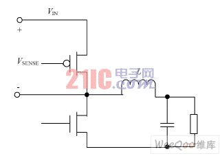
Figure 1 Current detection using the RDS of a power tube
2.2 Use of Sense Field Effect Transistor (SENSEFET)
This current sensing technology is more common in practical engineering applications. Its design concept is: As shown in Figure 2, a current sensing FET is connected in parallel at both ends of the power MOSFET. The effective width W of the sensing FET is significantly smaller than that of the power MOSFET. The effective width W of the power MOSFET should be more than 100 times that of the sensing FET (assuming that the effective lengths of the two are equal, the same below) to ensure that the additional power loss caused by the sensing FET is as small as possible. The currents of nodes S and M should be equal to avoid the inaccurate current mirror caused by the FET channel length effect.
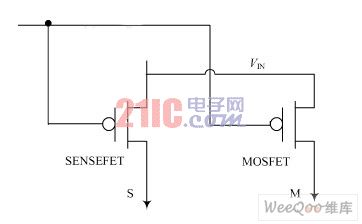
Figure 2 Current sensing using field effect transistors
When the potentials of nodes S and M are equal, the current IS flowing through the detection FET is 1/N of the power MOSFET current IM (N is the ratio of the width of the power FET to the detection FET), and the value of IS can reflect the size of IM.
2.3 Combination of detection field effect transistor and detection resistor
As shown in Figure 3, this detection technology is an improved form of the previous one, except that its detection device is not FET but a small resistor. In this detection circuit, the resistance value of the small resistor is relatively more accurate than the RDS of the detection FET, and its detection accuracy is relatively higher. In addition, there is no need for a special circuit to ensure that the voltage at the drain end of the power FET and the detection FET is equal, which reduces the design difficulty. However, the cost is that the additional power loss caused by the detection of the small resistor is smaller than 1/N2 of the first detection technology (N is the ratio of the width of the power FET and the detection FET). The disadvantage of this technology is that, because the V DS of M1 and M3 are not equal (considering the impact of VDS on IDS), the ratio of IM to IS is not strictly equal to N, but this deviation is relatively small. In engineering, N should be as large as possible and RSENSE should be as small as possible. This detection technology can be used in high-efficiency, low-voltage output, and large-load application environments.
[page]
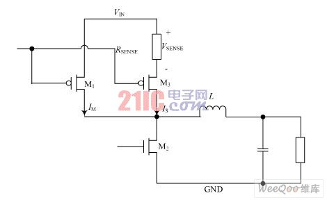
Figure 3 Field effect transistor combined with resistor for current detection
3 New current detection method
In Figure 4, N_DRV is the synchronous tube gate drive signal of the BUCK regulator, N_DRV_DC is the DC component filtered out by N_DRV after passing through a third-order RC low-pass filter, and the DC component is input to one end of the comparator, and the other end of the comparator is input to a reference voltage value BIAS3. The output LA28 of the comparator (digital signal, output to the control logic of the chip) is the DC2DC load current state detection signal.
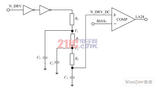
Figure 4: Equivalent architecture diagram of the basic principle of the new current detection method
The function of the current detection circuit is as follows:
In a voltage regulator chip, it includes both a DC2DC (BUCK) and an LDO. It works in PWM mode when medium and heavy loads are applied, and works in LDO when light loads (about 3 mA or less). The function of the current detection circuit proposed in this paper is: when its load current is less than a certain value (the switching regulator is in DCM mode at this time), the LA28 level jumps to realize the mode switching from PWM mode to LDO mode.
It should be noted here that if the output load current is directly detected or the output load current is detected by taking the average value of the inductor current, it will bring difficulties in circuit implementation. However, the detection method proposed here does not have this problem. The architecture diagram is an equivalent diagram of the DC2DC load current state detection circuit. Its function is that when the DC2DC load current is lower than 3 mA, its output signal LA28 changes from high to low, thereby realizing the switching from PWM mode to LDO. Its basic principle is to use the relationship between the load current and the switch gate drive signal N_DRV in DCM mode (when the load current is 3 mA, DC2DC is in DCM mode), and monitor the change of the output load current by detecting N_DRV, so as to switch from PWM mode to LDO when the load current is lower than 3 mA. The following will use Figure 5 to illustrate the principle of load current detection of this circuit.
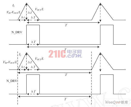
Figure 5 Basic principle of detecting DCDC load current
Figure 5 is a waveform diagram of the inductor current IL and the synchronous tube gate drive signal N_DRV in DCM mode.
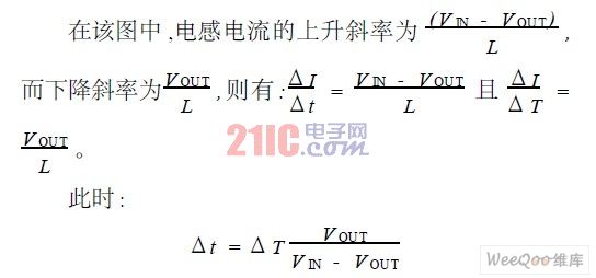
Since the amount of charge output to the load through the inductor in each cycle is constant, we have
 .
. Where: T is the switching period; IOUT is the output load current.
From the above formulas, we get:
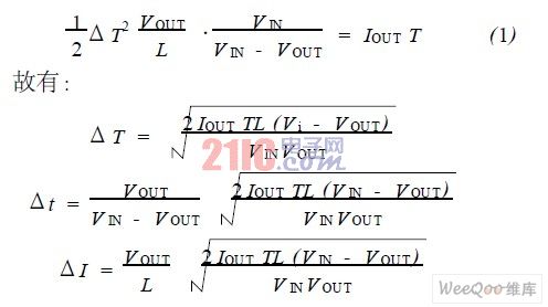
Now let's analyze Figure 4 again. In the frequency domain, the system transfer function from N_DRV to N_DRV_DC is:

Therefore, the network composed of R and C in Figure 4 is a third-order RC low-pass filter. Next, we calculate N_DRV_DC. From t = 0, we connect a periodic rectangular pulse signal N_DRV with a pulse width of ΔT and a period of T. Its image function in the complex frequency domain is Therefore,

the image function of N_DRV_DC is:

It should be noted that when designing a third-order RC low-pass filter, its bandwidth should be set much smaller than the oscillator frequency of DC2DC (i.e., the frequency of N_DRV) to ensure that the high-frequency components in N_DRV are well filtered out; but it should not be set too small, otherwise the resistance and capacitance used will be relatively large. [page]
When the DC2DC load current decreases, N_DRV_DC will also decrease. If it decreases to N_DRV_DC = BIAS3, the comparator starts to change from high to low, and the chip will enter the LDO mode from the PWM mode. Assume that the load current at this time is ILDO(ON), then:
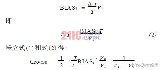
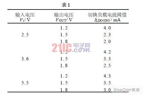
From the above formula, it can be seen that the switching threshold ILDO(ON) from DC2DC to LDO is inversely proportional to the inductance value L.
The final current detection circuit is shown in Figure 6. Since the circuit principle is relatively simple, the analysis is omitted.
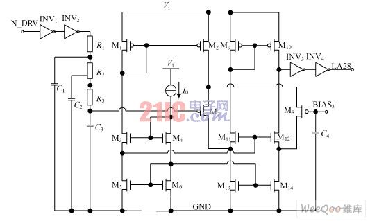
Figure 6 Final current detection implementation circuit
4 Simulation result data
The simulation result data is shown in Table 1. TA = 25 ℃, L = 2. 2μH.
5 Conclusion
A new method for current detection of switching regulator is proposed. By detecting the synchronous tube gate drive signal in DCM mode, the output load current is detected, so as to obtain the switching of the chip from PWM mode to LDO mode. This solves the difficulty of circuit implementation by detecting the average current of the inductor. After HSpice simulation verification, it only consumes 5μA of static current. This detection method is mainly suitable for occasions where the load current of the switching regulator in DCM mode needs to be detected.
Previous article:Design of attenuation systems for high power signal processing and testing
Next article:Design of an Intelligent Photoelectric Signal Acquisition and Analysis System
- Popular Resources
- Popular amplifiers
- Keysight Technologies Helps Samsung Electronics Successfully Validate FiRa® 2.0 Safe Distance Measurement Test Case
- From probes to power supplies, Tektronix is leading the way in comprehensive innovation in power electronics testing
- Seizing the Opportunities in the Chinese Application Market: NI's Challenges and Answers
- Tektronix Launches Breakthrough Power Measurement Tools to Accelerate Innovation as Global Electrification Accelerates
- Not all oscilloscopes are created equal: Why ADCs and low noise floor matter
- Enable TekHSI high-speed interface function to accelerate the remote transmission of waveform data
- How to measure the quality of soft start thyristor
- How to use a multimeter to judge whether a soft starter is good or bad
- What are the advantages and disadvantages of non-contact temperature sensors?
- Innolux's intelligent steer-by-wire solution makes cars smarter and safer
- 8051 MCU - Parity Check
- How to efficiently balance the sensitivity of tactile sensing interfaces
- What should I do if the servo motor shakes? What causes the servo motor to shake quickly?
- 【Brushless Motor】Analysis of three-phase BLDC motor and sharing of two popular development boards
- Midea Industrial Technology's subsidiaries Clou Electronics and Hekang New Energy jointly appeared at the Munich Battery Energy Storage Exhibition and Solar Energy Exhibition
- Guoxin Sichen | Application of ferroelectric memory PB85RS2MC in power battery management, with a capacity of 2M
- Analysis of common faults of frequency converter
- In a head-on competition with Qualcomm, what kind of cockpit products has Intel come up with?
- Dalian Rongke's all-vanadium liquid flow battery energy storage equipment industrialization project has entered the sprint stage before production
- Allegro MicroSystems Introduces Advanced Magnetic and Inductive Position Sensing Solutions at Electronica 2024
- Car key in the left hand, liveness detection radar in the right hand, UWB is imperative for cars!
- After a decade of rapid development, domestic CIS has entered the market
- Aegis Dagger Battery + Thor EM-i Super Hybrid, Geely New Energy has thrown out two "king bombs"
- A brief discussion on functional safety - fault, error, and failure
- In the smart car 2.0 cycle, these core industry chains are facing major opportunities!
- The United States and Japan are developing new batteries. CATL faces challenges? How should China's new energy battery industry respond?
- Murata launches high-precision 6-axis inertial sensor for automobiles
- Ford patents pre-charge alarm to help save costs and respond to emergencies
- New real-time microcontroller system from Texas Instruments enables smarter processing in automotive and industrial applications

 2005_High Frequency, High Current Density Voltage Regulator_Jinghai_Zhou


 京公网安备 11010802033920号