The current detection circuit is necessary for current mode control. It detects the current on the power switch tube, then outputs a current sensing signal to superimpose the slope compensation signal and convert it into a voltage signal, and then compares it with the output of the error amplifier, thereby realizing the control of the current inner loop of the current mode switch converter. There are many ways to implement it. There are two common methods. One is to connect a resistor Rsen in series with the power tube, and the other is to connect a parallel detection tube in parallel with the power tube to copy the proportional current. There are two main implementation structures for the detection method of the parallel detection tube copying the proportional current. One is to use the structure of the operational amplifier, and the other is to use the feedback method. If the operational amplifier is used, it will obviously increase the complexity of the circuit and increase the power consumption. This paper designs the feedback network in the current detection circuit based on the principle of feedback-controlled current source.
1 Principle of feedback-controlled current source
The circuit schematic diagram and the current source dynamic characteristic curve are shown in Figure 1 (a) and (b). According to the characteristic curve of the current source, the current characteristics of the relevant components in the bias circuit can only have a unique intersection (except the origin) when the linear and nonlinear current sources are combined, so as to ensure that the bias circuit has a unique stable operating point.
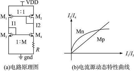
Figure 1 Schematic diagram of a current source with feedback control
Assume the voltage drop across the resistor is VR, the overdrive voltage of tube M3 is △, and based on the condition that the currents of M3 and M4 are equal, we get:

From this we can solve:

Among them, VR = VGS3 - V GS4, so the voltage difference of VGS determines the micro-current formed on the resistor, that is, the nonlinear relationship satisfied by the output current I0 is:

The output current thus solved is independent of the power supply voltage.
2 Specific circuit design and implementation of the current detection circuit
According to the previous analysis, it can be seen that when R is fixed, the circuit shown in Figure 1 can provide a unique bias current. However, in the current detection circuit, since the inductor current is always changing, it is obvious that a fixed resistor is no longer applicable. The improved circuit of Figure 1 is applied to the current detection circuit, as shown in Figure 2, where the resistor is replaced by a MOS tube MR working in the linear region.
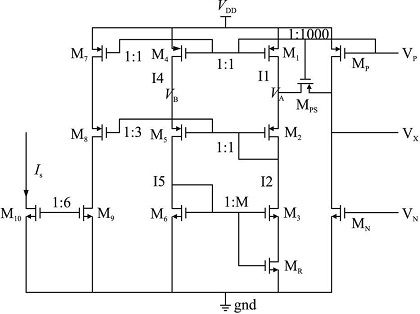
Figure 2 Improved current detection circuit with feedback-controlled current source For
MOS tubes operating in the linear region, the on-resistance rON can be obtained from the following formula:

It can be seen that rON is inversely proportional to VGS - VTH, so the resistance value will change with the change of VGS. In this way, the nonlinear current source formed by different resistance values combined with the current mirror will have different stable operating points. Therefore, in the whole work, for the inductor current that is constantly changing, the bias circuit achieves different dynamic stable states by changing the resistance value.
In order to achieve the accuracy of circuit detection, this paper uses a current source with feedback control and variable resistance value to replace the complex op amp.
In the current detection circuit shown in Figure 2, MP and MN are power tubes, M1 and M4, M2 and M5 have the same W/L, VP is the control signal of MP, and MPS is used as a switch, its W/L is relatively large and has a low on-resistance. In the current mode DC/DC converter, the feedback control loop only needs to detect the current when the MP power tube is turned on. Therefore, in order to reduce power consumption, the current detection circuit can be controlled to work only when the MP power tube is turned on, that is, only the current in the inductor charging stage is detected. When the MP power tube is turned off, the current detection circuit does not work, thereby effectively reducing power loss.
[page]
When VP is low, MP is turned on, and MPS is also turned on as a switch, and can be regarded as an approximate short circuit, and the current flowing through MPS can also be ignored. Therefore, the VDS of MP and M1 are approximately the same, and the current flowing through MP is mirrored to M1. MP is proportional to the W/L of M1, and the proportionality coefficient is large, so the detected current is proportional to the current in MP and is much smaller than the current in MP.
The relationship between VB and VA is analyzed below. Assuming that at a certain moment, the potential of VB is higher than VA, then VDS4 < VDS1, the current I4 in M4 is less than the current I1 in M1, and VDS5 > VDS2, requiring I5 > I2, which makes it impossible for I4 and I5 to be in the same branch, so VB will be the same as VA and maintain the same dynamic change. Therefore, the current in M1 is mirrored to M4 again, and due to the effect of feedback control current source, any small change at VA will force VB to have the same change, ensuring the accuracy of current detection.
According to the system design requirements, the current detection ratio should be K = 1 000:1. The circuit diagram shows the ratio of current replication at each level. Since the current detection circuit adopts a current source structure with feedback control and variable resistance value, it can be obtained that VA is equal to VB. Since the width-to-length ratio of M1, M4, and M7 is set equal, according to the MOS current formula, it can be obtained:

Detection accuracy and speed are two important indicators of the current detection circuit. Since the current detection circuit is in the startup state at the beginning of each detection cycle, Is has a startup time. This time is mainly determined by the parasitic capacitance of the M9 and M10 tubes in the circuit . When the width and length of the two tubes are relatively small, the startup time is very short. On the contrary, the startup time will become longer. In order to ensure the accuracy of current detection, the L of the M9 and M10 tubes cannot be too small, and 1 um is now taken.
3 Simulation results
By carefully adjusting the parameters of the MP tube and the M1 tube, the width-to-length ratio of the MP tube is set to 5 000 um/1 um, and the width-to-length ratio of the M1 tube is set to 5 um/1um. For the parameters of other tubes, refer to the proportional copy mark on the circuit diagram. Through the spetre simulation design tool in the Cadence software, the simulation verification is carried out at 25℃ using the CSMC 0.5 m CMOS
process. The simulation results of the current detection circuit are shown in Figure 3 below.
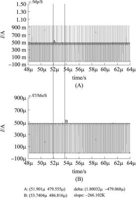
Figure 3 Simulation waveform of current detection circuit
From the measurement of the output waveform, it can be seen that when the maximum value of the inductor current IL is 479.55 A measured at point A, the maximum value of the detection current Is is 486.81 A measured at point B, which basically meets the following conditions:

Therefore, the designed current detection circuit can meet the design requirements well.
4 Conclusion
This paper designs a current detection circuit suitable for the DC/DC converter chip in the current mode, and designs the feedback network in the current detection circuit by using the principle of feedback-controlled current source. Through simulation verification, it can be seen that the designed circuit has good performance, and the sampling accuracy reaches 1 000:1, which fully meets the system design requirements.
Keywords:DC converter
Reference address:Design of Current Sensing Circuit in Current Mode Control DC/DC Converter
1 Principle of feedback-controlled current source
The circuit schematic diagram and the current source dynamic characteristic curve are shown in Figure 1 (a) and (b). According to the characteristic curve of the current source, the current characteristics of the relevant components in the bias circuit can only have a unique intersection (except the origin) when the linear and nonlinear current sources are combined, so as to ensure that the bias circuit has a unique stable operating point.

Figure 1 Schematic diagram of a current source with feedback control
Assume the voltage drop across the resistor is VR, the overdrive voltage of tube M3 is △, and based on the condition that the currents of M3 and M4 are equal, we get:

From this we can solve:

Among them, VR = VGS3 - V GS4, so the voltage difference of VGS determines the micro-current formed on the resistor, that is, the nonlinear relationship satisfied by the output current I0 is:

The output current thus solved is independent of the power supply voltage.
2 Specific circuit design and implementation of the current detection circuit
According to the previous analysis, it can be seen that when R is fixed, the circuit shown in Figure 1 can provide a unique bias current. However, in the current detection circuit, since the inductor current is always changing, it is obvious that a fixed resistor is no longer applicable. The improved circuit of Figure 1 is applied to the current detection circuit, as shown in Figure 2, where the resistor is replaced by a MOS tube MR working in the linear region.

Figure 2 Improved current detection circuit with feedback-controlled current source For
MOS tubes operating in the linear region, the on-resistance rON can be obtained from the following formula:

It can be seen that rON is inversely proportional to VGS - VTH, so the resistance value will change with the change of VGS. In this way, the nonlinear current source formed by different resistance values combined with the current mirror will have different stable operating points. Therefore, in the whole work, for the inductor current that is constantly changing, the bias circuit achieves different dynamic stable states by changing the resistance value.
In order to achieve the accuracy of circuit detection, this paper uses a current source with feedback control and variable resistance value to replace the complex op amp.
In the current detection circuit shown in Figure 2, MP and MN are power tubes, M1 and M4, M2 and M5 have the same W/L, VP is the control signal of MP, and MPS is used as a switch, its W/L is relatively large and has a low on-resistance. In the current mode DC/DC converter, the feedback control loop only needs to detect the current when the MP power tube is turned on. Therefore, in order to reduce power consumption, the current detection circuit can be controlled to work only when the MP power tube is turned on, that is, only the current in the inductor charging stage is detected. When the MP power tube is turned off, the current detection circuit does not work, thereby effectively reducing power loss.
[page]
When VP is low, MP is turned on, and MPS is also turned on as a switch, and can be regarded as an approximate short circuit, and the current flowing through MPS can also be ignored. Therefore, the VDS of MP and M1 are approximately the same, and the current flowing through MP is mirrored to M1. MP is proportional to the W/L of M1, and the proportionality coefficient is large, so the detected current is proportional to the current in MP and is much smaller than the current in MP.
The relationship between VB and VA is analyzed below. Assuming that at a certain moment, the potential of VB is higher than VA, then VDS4 < VDS1, the current I4 in M4 is less than the current I1 in M1, and VDS5 > VDS2, requiring I5 > I2, which makes it impossible for I4 and I5 to be in the same branch, so VB will be the same as VA and maintain the same dynamic change. Therefore, the current in M1 is mirrored to M4 again, and due to the effect of feedback control current source, any small change at VA will force VB to have the same change, ensuring the accuracy of current detection.
According to the system design requirements, the current detection ratio should be K = 1 000:1. The circuit diagram shows the ratio of current replication at each level. Since the current detection circuit adopts a current source structure with feedback control and variable resistance value, it can be obtained that VA is equal to VB. Since the width-to-length ratio of M1, M4, and M7 is set equal, according to the MOS current formula, it can be obtained:

Detection accuracy and speed are two important indicators of the current detection circuit. Since the current detection circuit is in the startup state at the beginning of each detection cycle, Is has a startup time. This time is mainly determined by the parasitic capacitance of the M9 and M10 tubes in the circuit . When the width and length of the two tubes are relatively small, the startup time is very short. On the contrary, the startup time will become longer. In order to ensure the accuracy of current detection, the L of the M9 and M10 tubes cannot be too small, and 1 um is now taken.
3 Simulation results
By carefully adjusting the parameters of the MP tube and the M1 tube, the width-to-length ratio of the MP tube is set to 5 000 um/1 um, and the width-to-length ratio of the M1 tube is set to 5 um/1um. For the parameters of other tubes, refer to the proportional copy mark on the circuit diagram. Through the spetre simulation design tool in the Cadence software, the simulation verification is carried out at 25℃ using the CSMC 0.5 m CMOS
process. The simulation results of the current detection circuit are shown in Figure 3 below.

Figure 3 Simulation waveform of current detection circuit
From the measurement of the output waveform, it can be seen that when the maximum value of the inductor current IL is 479.55 A measured at point A, the maximum value of the detection current Is is 486.81 A measured at point B, which basically meets the following conditions:

Therefore, the designed current detection circuit can meet the design requirements well.
4 Conclusion
This paper designs a current detection circuit suitable for the DC/DC converter chip in the current mode, and designs the feedback network in the current detection circuit by using the principle of feedback-controlled current source. Through simulation verification, it can be seen that the designed circuit has good performance, and the sampling accuracy reaches 1 000:1, which fully meets the system design requirements.
Previous article:Application of MDO mixed domain oscilloscope in IoT design, development and training
Next article:The Principle and Maintenance Method of Dual-Trace Oscilloscope
- Popular Resources
- Popular amplifiers
Recommended Content
Latest Test Measurement Articles
- New IsoVu™ Isolated Current Probes: Bringing a New Dimension to Current Measurements
- Modern manufacturing strategies drive continuous improvement in ICT online testing
- Methods for Correlation of Contact and Non-Contact Measurements
- Keysight Technologies Helps Samsung Electronics Successfully Validate FiRa® 2.0 Safe Distance Measurement Test Case
- From probes to power supplies, Tektronix is leading the way in comprehensive innovation in power electronics testing
- Seizing the Opportunities in the Chinese Application Market: NI's Challenges and Answers
- Tektronix Launches Breakthrough Power Measurement Tools to Accelerate Innovation as Global Electrification Accelerates
- Not all oscilloscopes are created equal: Why ADCs and low noise floor matter
- Enable TekHSI high-speed interface function to accelerate the remote transmission of waveform data
MoreSelected Circuit Diagrams
MorePopular Articles
- Intel promotes AI with multi-dimensional efforts in technology, application, and ecology
- ChinaJoy Qualcomm Snapdragon Theme Pavilion takes you to experience the new changes in digital entertainment in the 5G era
- Infineon's latest generation IGBT technology platform enables precise control of speed and position
- Two test methods for LED lighting life
- Don't Let Lightning Induced Surges Scare You
- Application of brushless motor controller ML4425/4426
- Easy identification of LED power supply quality
- World's first integrated photovoltaic solar system completed in Israel
- Sliding window mean filter for avr microcontroller AD conversion
- What does call mean in the detailed explanation of ABB robot programming instructions?
MoreDaily News
- USB Type-C® and USB Power Delivery: Designed for extended power range and battery-powered systems
- RAQ #223: How to measure and determine soft-start timing without a soft-start equation?
- RAQ #223: How to measure and determine soft-start timing without a soft-start equation?
- GigaDevice's full range of automotive-grade SPI NOR Flash GD25/55 wins ISO 26262 ASIL D functional safety certification
- GigaDevice's full range of automotive-grade SPI NOR Flash GD25/55 wins ISO 26262 ASIL D functional safety certification
- New IsoVu™ Isolated Current Probes: Bringing a New Dimension to Current Measurements
- New IsoVu™ Isolated Current Probes: Bringing a New Dimension to Current Measurements
- Infineon Technologies Launches ModusToolbox™ Motor Kit to Simplify Motor Control Development
- Infineon Technologies Launches ModusToolbox™ Motor Kit to Simplify Motor Control Development
- STMicroelectronics IO-Link Actuator Board Brings Turnkey Reference Design to Industrial Monitoring and Equipment Manufacturers
Guess you like
- Optimizing DSP Power Budget by Adjusting Voltage Regulators
- WiMAX certification process and its significance to network operators and suppliers
- Rapoo Multi-mode Bluetooth Mouse M600 Disassembly
- Comparison between DSP processor and general processor
- Reduce the allegro brd layout file version from 17.2 to 16.6
- PhD thesis - Pattern tracking rules based on integral variable structures
- Protel/AD design software removes text
- Application of DSP Digital Signal Processor in Coriolis Mass Flow Meter
- Selection and application of backlight drive circuit
- Let's discuss

 5962-9153202Q2A


 京公网安备 11010802033920号