2.3 Extraction principle and simulation of MRS signal
2.3.1 Extraction of MRS signal parameters
The ground NMR water search signal expression is:
Where E 0 is the initial amplitude, ω 0 is the Lamor angular frequency, θ is the initial phase, and T 2 * is the relaxation time. Since the Lamor frequency of the signal can be calculated based on the magnitude of the geomagnetic field in nuclear magnetic resonance water detection, and the signal is a single-frequency signal, the orthogonal vector amplification method can be used to detect and extract its envelope curve:
Thus, various parameters of the MRS signal such as E 0 , T 2 * , and θ are obtained.
We assume that the MRS signal after passing through the signal channel is:
n(t) is the noise.
δ ω =ω 0 -ω 1 is the frequency difference.
The signal is multiplied by the phase sensitive detector PSD:
Then pass through the low-pass filter LPF to filter out the high-frequency part and get:
After mathematical calculation of I(t) and Q(t):

After data fitting, the parameters of MRS signal such as E 0 , T 2 * , θ, etc. can be obtained.
2.3.2 MATLAB simulation
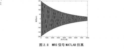
The entire MRS signal envelope extraction process can be simulated using MATLAB. Assume that the initial amplitude of the MRS signal is E 0 = 200mV, the Lamor frequency is f 0 = 2300Hz, the initial phase is θ = π/3, and the relaxation time is T 2 * = 100ms. The standard MRS signal can be obtained as shown in Figure 2.8.
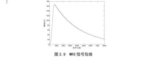
After multiplying with the sine and cosine reference signals of the same frequency and passing through a digital low-pass filter (the cut-off frequency is set to 10 Hz), the envelope of the standard MRS signal can be obtained as shown in Figure 2.9.
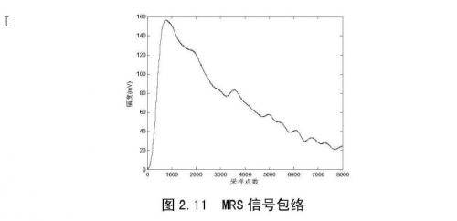
In actual measurement, the MRS signal is accompanied by a certain amount of noise, and the reference signal cannot be completely at the same frequency as the MRS signal. Figures 2.10 and 2.11 show the waveform of the MRS signal containing Gaussian white noise (signal-to-noise ratio is 0.6) and the signal envelope obtained after orthogonalization with a sine wave with a frequency of 2290Hz. It can be seen that the orthogonal vector amplification method used in this design can well improve the signal-to-noise ratio.
After fitting the data shown in equations (2-18) and (2-19), the fitting results are shown in Table 2.1.
The simulation verifies that the orthogonal vector amplification method can accurately extract the characteristic parameters of the signal and further improve the signal-to-noise ratio. This method allows a certain deviation between the frequency of the reference signal and the measured signal, and the smaller the deviation, the better. [page]
Chapter 3 Collection Module Design
3.1 Overall structure of the NMR water detector
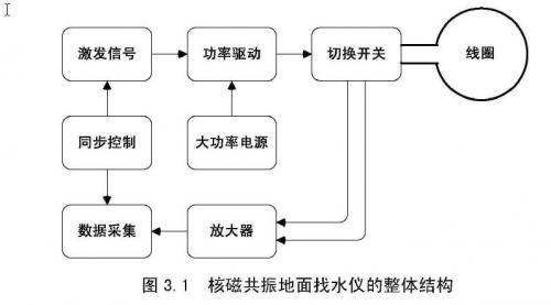
The nuclear magnetic resonance water detector consists of a power supply, transmitting and receiving parts, as shown in Figure 3.1.
Under computer control, the single-chip microcomputer and DDS generate the Larmor excitation signal shown in Figure 3.2 (a). The power driving circuit modulates this signal into the current required for emission, and transmits the excitation signal through the switch through the cable laid on the ground. After the excitation stops, the cable is connected to the input of the amplifier by the fast switch control circuit. The amplifier performs analog conditioning on the received MRS signal shown in Figure 3.2 (b) and outputs it to the data acquisition and processing circuit, which becomes the detected groundwater information after data processing. The data acquisition module in Figure 3.1 is the main research content of this paper.
3.2 Main functions and design indicators of the acquisition module
3.2.1 Main functions of the acquisition module
1. Generate two reference sine waves with the same frequency as the MRS signal, with a phase difference of 90°;
2. Realize orthogonal vector amplification of two reference signals and MRS signals;
3. Synchronously collect two orthogonal signals;
4. Use the communication module to receive the host computer's instructions and upload the collected data to the host computer;
5. The host computer software processes the received data and displays it in a graph.
3.2.2 Technical indicators of the acquisition module
ADC bit number: 16 bits
Acquisition channel: 2 channels synchronous acquisition
Signal input range: -2.5V~+2.5V
Sampling rate: adjustable by 1/4 Lamor frequency
Sampling time: 0ms~500ms programmable
3.3 Design Block Diagram
3.3.1 Implementation of the main circuit
In this design, the 51 series single-chip microcomputer is used as the control core to control data collection and processing. This design adopts the envelope collection scheme, and the amount of data collected is small. The 51 series single-chip microcomputer can meet the requirements of speed and capacity. In addition, the 51 series single-chip microcomputer also has the advantages of complete development environment, complete development tools, mature application technology, stable and reliable operation, and economical price.
Nowadays, the technology of programmable logic device CPLD is quite mature. CPLD devices have excellent high-speed performance, high flexibility, reliability, large-scale integration and in-system programmability. At the same time, the price of CPLD is also very cheap, with a high cost performance.
After comprehensive consideration, this design adopts the solution of single-chip microcomputer plus CPLD. The perfect combination of single-chip microcomputer and CPLD also takes the application of single-chip microcomputer to a higher level, integrating many complex hardware circuits on a chip, greatly reducing the difficulty of wiring and simplifying the circuit. The phase-sensitive detector PSD is a relatively important part of the system and also a relatively complex part in the circuit design. In this system, CPLD and multiplication type D/A converter are selected to form an analog multiplication type phase-sensitive detector. The multiplication type D/A converter has digital input, reference voltage input, and analog output. The working principle is shown in Figure 3.3.
The output of the D/A converter is:
The waveform of the sine wave stored in CPLD is input into the digital input of the D/A converter, and the MRS signal after the nuclear magnetic resonance amplifier is input into the reference voltage input of the D/A converter. The multiplication result of the two will be obtained at the analog output. In this way, the generation of the sine wave signal and the multiplication with the MRS signal are realized by a simple circuit, realizing the function of the phase-sensitive detector. The
nuclear magnetic resonance amplifier in front of the acquisition module realizes the function of the signal channel. The nuclear magnetic resonance amplifier has the advantages of low noise, high gain, adjustable center frequency and gain, which can well meet the requirements of the signal channel. The frequency, amplitude and phase of the sine wave signal generated by the CPLD can be programmed and adjusted by the host computer, generating a reference signal and realizing the function of the reference channel.
3.3.2 Overall block diagram
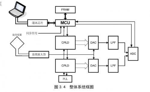
The overall circuit block diagram is shown in Figure 3.4. The entire system is controlled by a single-chip microcomputer and then operated by the host computer through a 485 communication chip. After the signal passes through the phase-sensitive detector, it is collected through an A/D converter under the sampling timing control generated by the CPLD. The collected I and Q data are sent to the host computer for processing through the single-chip microcomputer. The capacity of the internal memory of the single-chip microcomputer is limited. The collected data needs to be stored in the external memory FRAM first, and then transmitted to the host computer when the host computer needs it. The phase-locked loop PLL plays a frequency multiplication role in order to output a more accurate frequency sinusoidal reference signal. The start acquisition time, sampling rate, and acquisition end time of the entire acquisition module can be controlled by the host computer.
Previous article:Design of MRS signal acquisition module based on orthogonal vector amplification ---- Actual measurement results of acquisition module
Next article:Research on the low-frequency noise test technology and application of high-resistance devices--Study on leakage current noise of polymer tantalum capacitors
- Popular Resources
- Popular amplifiers
-
 TOWARDS CMOS NUCLEAR MAGNETIC RESONANCE SPECTROSCOPY DESIGN, IMPLEMENTATION AND EXPERIMENTAL RESULTS
 -
 Nuclear Magnetic Resonance (NMR) Spectroscopy for the In Situ Measurement of Vapor−Liquid Equilibria
 -
 Beta‐detected Nuclear Magnetic Resonance (β‐NMR) Towards Depth Resolved NMR
 -
 Measuring display part of nuclear magnetic resonance field measuring instrument
- Keysight Technologies Helps Samsung Electronics Successfully Validate FiRa® 2.0 Safe Distance Measurement Test Case
- From probes to power supplies, Tektronix is leading the way in comprehensive innovation in power electronics testing
- Seizing the Opportunities in the Chinese Application Market: NI's Challenges and Answers
- Tektronix Launches Breakthrough Power Measurement Tools to Accelerate Innovation as Global Electrification Accelerates
- Not all oscilloscopes are created equal: Why ADCs and low noise floor matter
- Enable TekHSI high-speed interface function to accelerate the remote transmission of waveform data
- How to measure the quality of soft start thyristor
- How to use a multimeter to judge whether a soft starter is good or bad
- What are the advantages and disadvantages of non-contact temperature sensors?
- Innolux's intelligent steer-by-wire solution makes cars smarter and safer
- 8051 MCU - Parity Check
- How to efficiently balance the sensitivity of tactile sensing interfaces
- What should I do if the servo motor shakes? What causes the servo motor to shake quickly?
- 【Brushless Motor】Analysis of three-phase BLDC motor and sharing of two popular development boards
- Midea Industrial Technology's subsidiaries Clou Electronics and Hekang New Energy jointly appeared at the Munich Battery Energy Storage Exhibition and Solar Energy Exhibition
- Guoxin Sichen | Application of ferroelectric memory PB85RS2MC in power battery management, with a capacity of 2M
- Analysis of common faults of frequency converter
- In a head-on competition with Qualcomm, what kind of cockpit products has Intel come up with?
- Dalian Rongke's all-vanadium liquid flow battery energy storage equipment industrialization project has entered the sprint stage before production
- Allegro MicroSystems Introduces Advanced Magnetic and Inductive Position Sensing Solutions at Electronica 2024
- Car key in the left hand, liveness detection radar in the right hand, UWB is imperative for cars!
- After a decade of rapid development, domestic CIS has entered the market
- Aegis Dagger Battery + Thor EM-i Super Hybrid, Geely New Energy has thrown out two "king bombs"
- A brief discussion on functional safety - fault, error, and failure
- In the smart car 2.0 cycle, these core industry chains are facing major opportunities!
- The United States and Japan are developing new batteries. CATL faces challenges? How should China's new energy battery industry respond?
- Murata launches high-precision 6-axis inertial sensor for automobiles
- Ford patents pre-charge alarm to help save costs and respond to emergencies
- New real-time microcontroller system from Texas Instruments enables smarter processing in automotive and industrial applications
- BleFi - BLE Wifi IOT Gateway Reference Design
- About the selection of energy storage inductor in DCDC circuit?
- [Analog Electronics Course Selection Test] + Assessment
- Matrix keyboard problem
- [Raspberry Pi Pico Review] 5. Pico drives LCD1602
- DIY Extended WiFi Antenna
- Characteristics and Applications of Voltage Monitoring Chip TPS383X
- 5G signal improvements could save $193 million per US fixed-access O-RAN network
- How to analyze which solution is better when two rectifier bridges are connected together?
- [RVB2601 Creative Application Development] Introduction and use of RVB2601 WiFi networking to obtain weather information






 TOWARDS CMOS NUCLEAR MAGNETIC RESONANCE SPECTROSCOPY DESIGN, IMPLEMENTATION AND EXPERIMENTAL RESULTS


 京公网安备 11010802033920号