The design of signal conditioning platform is an important part of building a large-scale missile test system based on VXI bus, and it is also the primary task of its hardware implementation. At present, the increase in the types, scale and complexity of large-scale missile equipment has brought new challenges to the design of the signal conditioning platform of the test equipment. If a dedicated signal conditioning platform is designed for different types of large-scale missile equipment, the workload is huge, repeated development is serious, and the economic price is low, which is not conducive to the formation of generalization, standardization and serialization of equipment. The emergence of in-system programmability (ISP) technology represents the development direction of the new generation of PLD. It provides the possibility of on-site system reconstruction and on-site system customization, making remote control on-site upgrade and maintenance possible. It is very suitable to use it to realize the programmable control unit of the signal transfer module. To this end, this paper designs a universal signal conditioning platform for large-scale missile test system based on ISP to meet the test requirements of different types of missiles.
1 ISP Technology
Programmable Logic Device (PLD) was born in the 1970s. It is a new type of logic device that can be programmed by the user to achieve a specific function. Since its inception, it has experienced a development process from low-density PLDs such as PROM, PLA, PAL, GAL to high-density PLDs such as CPLD and FPLD. At present, the integration of devices is getting higher and higher, and the functions are constantly enhanced. The number of logic gates has increased from 5,000 to 1,000.
The number of gates increased to 2 million, and some even reached tens of millions. The ISP technology that appeared in 1991 provided new development space for PLD and represented the development direction of the new generation of PLD technology. It has the following main features:
(1) Shortened the system design and trial production cycle and reduced the trial production cost;
(2) Reduced chip size and simplified production process;
(3) It facilitates system maintenance and upgrade;
(4) Improved the testability of the system and increased the reliability of the system.
The development of ISP devices does not require a programmer, and the logic function code can be directly downloaded to the device through a cable. VHDL language, as the mainstream development platform, has been formulated by IEEE as the IEEE1076.3 standard. It uses a specific syntax to describe the logic function of the device, providing a convenient development tool for on-site system reconstruction and function customization, simplifying system design.
2 Signal Conditioning Platform
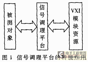
The signal conditioning platform is the intermediate link between the back-end large missile equipment test object and the front-end VXI module resources, as shown in Figure 1. Its functions mainly include the following two points: First, in terms of the test object, it realizes the distribution and transfer of the test signal on the conditioning bus, as well as the amplification, isolation, filtering and other transformations in the conditioning module, providing clean and stable test signals to the VXI test resources. Second, in terms of VXI module resources, it is responsible for transmitting power signals and excitation signals to the test object, connecting and switching the test signal with the test object, and maintaining maximum compatibility with the VXI electrical specifications.

3 Implementation of the signal conditioning platform
3.1 Hardware Framework
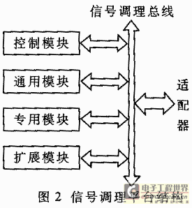
The signal conditioning platform adopts the structure of "adapter + signal conditioning bus + signal conditioning module", as shown in Figure 2. The adapter aggregates the measured signal, test signal and stimulus signal, and transmits them to the signal conditioning bus. The platform integration is achieved by plugging the plug-and-play signal conditioning module on the standardized electrical-independent signal conditioning bus. [page]

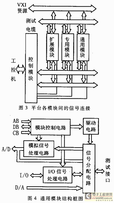
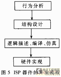
In order to improve the universality and standardization of the signal conditioning platform, the conditioning circuit is divided into control module, general module, special module and extension module. It adopts a standard card structure, forms a plug-in structure with the signal conditioning bus through a 96-pin DIN connector, and is fixed in an embedded chassis. The connection relationship between the modules is shown in Figure 3. The control module receives instructions from the digital I/O card of the industrial computer and implements program control management for the entire conditioning platform; the general module mainly completes dynamic allocation and preprocessing of the test signal, and the internal circuit includes module control circuit, signal distribution circuit, analog signal processing circuit, I/O signal processing circuit, etc. The structure is shown in Figure 4; the special module realizes some special functions, such as channel self-test, special signal conditioning when testing certain objects under test, etc.; the extension module is used for system function expansion.

3.2 Signal conditioning module design
3.2.1 Selection of ISP Devices
The general signal conditioning platform does not have high requirements for the scale of ISP devices, but requires reliable performance, flexible development, strong reconstruction ability and good versatility. Lattice's ispLSI series, Altera's 7000S and 9000 series, and Xilinx's XC9500 series are more commonly used ISP devices. Among them, Lattice is the first to propose ISP and has relatively mature technology in this regard. Its ISP chips belong to small and medium-sized CLPDs, including 6 series, with rich product varieties, low prices, flexible development, and can be directly applied to the system; the development platforms ispDesign EXPERT and PACDesigner are powerful and easy to use. The company also took the lead in launching the in-system programmable analog device (ispPAC) in 1999, which brought a revolutionary breakthrough in the interface design of analog circuits. For this reason, the control circuit and digital signal conditioning circuit of the signal conditioning platform in this article are implemented using Lattice's ispLSI032, and the analog signal conditioning circuit is implemented using ispPAC20.
.
3.2.2 Design Process
The design of the signal conditioning module in this system includes two parts: the functional design of the ISP device and the design of the peripheral circuit of the ISP device. The functional design of the ISP device is the main one, which determines the design of its peripheral circuit.
The functional design of ISP devices is also divided into two parts: the digital part based on the ispDesign EXPERT platform - the functional design of ispLSI1032 and the analog part based on the PAC-Designer platform - the functional design of ispPAC20. The design process of ISP devices is shown in Figure 5. Among them, "behavior analysis" determines the functions and index requirements to be completed by the device, and defines the input and output signals; "structural design" determines the implementation details of the system functions, gives the flowchart of the system design and describes the functions in VHDL language, and gives the timing diagram of the system when necessary; "logic description" is to implement the structural design with ispDesign EXPERT and PAC-Designer software, compile and simulate, verify the design results, and generate a download file - JEDEC; "hardware implementation" is to design and complete the specific circuit based on the previous work, including the design of the circuit board, the welding of the device, the download of the JEDEC file to the ISP device, and the joint debugging of the system functions.
4 Working process of signal conditioning platform application
When the platform is integrated with a certain type of missile test system, it is only necessary to design a dedicated signal conditioning module based on the test requirements of the missile, and distribute the measured signal, test signal and excitation signal to the signal conditioning bus through its adapter, and then realize convenient integration with the missile test system by programming the control signal transfer.
During the test, the control command from the digital I/O card of the main control computer is sent to the control module via the conditioning bus. After being decoded by the control module, the corresponding conditioning module is controlled to act so that the target signal of the path is transferred. The main control computer selects the path through the multi-way switch module of the VXI bus.
The test is completed. The excitation process is the opposite.
5. Several key issues in the process of platform universal design
In order to make the platform have good versatility, the following indicators must be met: the signal conditioning bus is standardized and electrical characteristics are independent; the plug-and-play signal conditioning circuit is programmable, modular, and channel management is automated; the entire platform has scalability. [page]
5.1 Standardization and Electrically Independent Design of the Conditioning Bus
The signal conditioning bus is the channel connecting the object under test, VXI resources and signal conditioning modules. Its standardized and electrically independent design is the basic indicator requirement for a universal and standardized signal conditioning platform. The signal conditioning bus is strictly defined based on the demand analysis of various types of large missiles under test and the functional definition of VXI test resources. It is mainly composed of a conditioning control bus and a data transmission bus. The conditioning control bus transmits the control instructions from the digital I/O card of the industrial computer to the control module, and controls the operation of the entire platform after decoding; the data transmission bus constitutes the connection channel between the measured signal, the conditioning module and the VXI resource (see Figure 3). Under the premise of strict definition of the bus, the selection and layout of the connection sockets, the connection method of the signal, and the definition of the connection status must fully consider electromagnetic compatibility. For this reason, this platform adopts the "bottom plate + backplane" (bottom plate adaptation, backplane conditioning) structure in the embedded chassis to isolate the adapter and the conditioning bus to make the signal transfer space as large as possible; and a ground layer is specially added to the circuit board design of the bottom plate and the back plate to separate the analog ground, digital ground, power ground and test signal, so that the excitation signal and the test signal can run in a clean and unobstructed transmission channel to minimize interference.
5.2 Programmable and modular design of conditioning circuits
Modularization and program control are the development direction of the test system. Designing a program control and analog signal conditioning platform is an objective requirement to achieve the versatility of the platform. In the process of conditioning circuit design, the modular design concept of "control module + energy module + special module + expansion module" is adopted. These modules and the conditioning bus form a plug-in structure (see Figure 2). The control unit and digital switching circuit of each module are implemented by ispSL1032, and the analog switching circuit is implemented by ispPAC20. The external interface is connected to the conditioning control bus and can be programmed. The general module realizes most of the conditioning functions of the test system, and the special module corresponds to different test objects and test tasks. When building large missile test systems of different models, system integration can be achieved by increasing or decreasing the number of general modules and designing different special modules.

5.3 Automated design of channel management for plug-and-play conditioning modules
The management of signal conditioning channels is a key step to improve the intelligence of general signal conditioning platforms, including the establishment and cancellation of channels (electrical interconnection of ports), control and monitoring of channel status, which is generally achieved by directly controlling the status of the channel management unit - ISP device. Therefore, the measurement and control software is inseparable from the conditioning circuit control unit. To achieve automatic management of signal conditioning circuits, the measurement and control conditioning circuit control should be based on the signal transmission characteristics of each channel in the conditioning circuit.
Here, the management of conditioning circuit channels is divided into three independent files: interface configuration, control function and control model. The interface configuration file stores the interface mapping information between the object under test and the test resources and the channel conditioning parameters, which can be developed through the software development platform (such as Labwindows/CVI
The universal signal conditioning platform has been applied in the universal maintenance and inspection system of the army's missile equipment. Experiments have proved that it can meet the index requirements of different test objects and different test tasks, with high universality and standardization, and strong expansion capability.
Previous article:Sensing-based measurement of low-Q inductors
Next article:Application Design of VHDL in High-speed Image Acquisition System
- Keysight Technologies Helps Samsung Electronics Successfully Validate FiRa® 2.0 Safe Distance Measurement Test Case
- From probes to power supplies, Tektronix is leading the way in comprehensive innovation in power electronics testing
- Seizing the Opportunities in the Chinese Application Market: NI's Challenges and Answers
- Tektronix Launches Breakthrough Power Measurement Tools to Accelerate Innovation as Global Electrification Accelerates
- Not all oscilloscopes are created equal: Why ADCs and low noise floor matter
- Enable TekHSI high-speed interface function to accelerate the remote transmission of waveform data
- How to measure the quality of soft start thyristor
- How to use a multimeter to judge whether a soft starter is good or bad
- What are the advantages and disadvantages of non-contact temperature sensors?
- Innolux's intelligent steer-by-wire solution makes cars smarter and safer
- 8051 MCU - Parity Check
- How to efficiently balance the sensitivity of tactile sensing interfaces
- What should I do if the servo motor shakes? What causes the servo motor to shake quickly?
- 【Brushless Motor】Analysis of three-phase BLDC motor and sharing of two popular development boards
- Midea Industrial Technology's subsidiaries Clou Electronics and Hekang New Energy jointly appeared at the Munich Battery Energy Storage Exhibition and Solar Energy Exhibition
- Guoxin Sichen | Application of ferroelectric memory PB85RS2MC in power battery management, with a capacity of 2M
- Analysis of common faults of frequency converter
- In a head-on competition with Qualcomm, what kind of cockpit products has Intel come up with?
- Dalian Rongke's all-vanadium liquid flow battery energy storage equipment industrialization project has entered the sprint stage before production
- Allegro MicroSystems Introduces Advanced Magnetic and Inductive Position Sensing Solutions at Electronica 2024
- Car key in the left hand, liveness detection radar in the right hand, UWB is imperative for cars!
- After a decade of rapid development, domestic CIS has entered the market
- Aegis Dagger Battery + Thor EM-i Super Hybrid, Geely New Energy has thrown out two "king bombs"
- A brief discussion on functional safety - fault, error, and failure
- In the smart car 2.0 cycle, these core industry chains are facing major opportunities!
- The United States and Japan are developing new batteries. CATL faces challenges? How should China's new energy battery industry respond?
- Murata launches high-precision 6-axis inertial sensor for automobiles
- Ford patents pre-charge alarm to help save costs and respond to emergencies
- New real-time microcontroller system from Texas Instruments enables smarter processing in automotive and industrial applications
- Arteli AT32F4xx Standard Peripheral Library Release Notes
- AD 3D component package library
- "Vivado Starts Here" - Quickly Get Started with Vivado
- If the PCB heat dissipation area is not enough, will increasing the copper thickness help improve the heat dissipation of the PCB?
- Can't tell the difference? The difference between RF analog signal source and vector signal source
- Most EMI problems are related to clock signals.
- Share: AD batch hide component labels
- [Xiao Meige SoC] How to view the number of GPIO added on the FPGA side of the SoC FPGA system and use interrupts
- What are the two parts of RFID?
- How to use the virtual serial port VCOM function of J-Link?

 Digilent Vivado library
 Fundamentals of Radar Signal Processing(Second Edition)


 京公网安备 11010802033920号