In this article we will analyze the need for measuring power in some modern communications systems and introduce power measurement techniques as well as the errors and uncertainties that exist in the process of making power measurements.
Customer demand for ever-increasing data rates has driven a move from simple constant-envelope modulation schemes used in first-generation mobile phones and microwave links—such as FM used in PMR equipment—to more complex modulation schemes such as GMSK, CDMA, and N-QAM.
This article will focus on root mean square (RMS) measurements for CDMA and N-QAM systems and will introduce two different types of sensor technologies that can be used to measure these types of signals.
CDMA signals such as IS-95 (the North American narrowband CDMA standard) or the 3GPP WCDMA standard have a lot of amplitude content. Typically, the peak-to-average power ratio is a minimum of 10dB and can be as high as 16dB. This amplitude variation makes traditional CW linearity-corrected diode sensors unsuitable for these types of measurements.
RF links have adopted N-QAM—typically 64 QAM or 256 QAM—modulation to increase data rates. Other newer, higher data rate systems such as WLAN standards also use 64QAM to achieve the fastest data rates. The symbol rates of these systems are usually higher than the bandwidth of most common peak power meters, and RMS measurements can give an accurate and economical indication of the system's power.
Power measurement technology has identified three main categories of power sensor designs: thermistors, diodes, and thermopiles or Seebeck effect. Thermistors have traditionally been used for standard conversions and are not used for routine measurements of systems and devices because of their limited power handling capabilities.
Diode-based sensors have always come in two different flavors: square-law-only sensors and linear-corrected wide dynamic range sensors. Recently, a third class of diode sensors has been introduced, those based on multiple diodes.
Thermopile or Seebeck effect sensors work on the principle of thermocouples and rely on the thermal effect of the input signal. This makes them ideal for measuring the true RMS power of complex waveforms such as N-QAM, because they will always respond to the true RMS value of the input waveform regardless of the modulation method applied to the carrier.
Thermopiles have good return loss, which reduces measurement uncertainty. The only drawback is that they have a limited dynamic range and a slower response time than diode sensors. Anritsu's fast thermal sensors have a 4ms response time.
Figure 2 shows the responses of the thermopile cell and diode detector. Conventional diode detectors either operate in the square law region, limiting their dynamic range to 50 dB, or use linear correction techniques to extend their dynamic range. This technique is limited by the speed of the power meter and is not suitable for applications where the symbol rate of the system transmission far exceeds the power meter sampling rate.
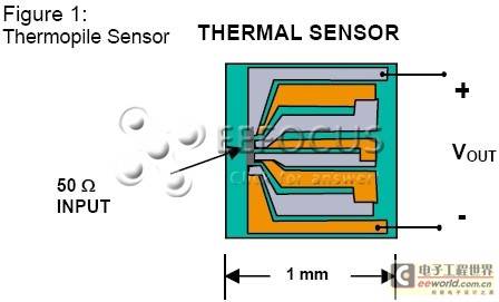
Figure 1: Thermopile sensor
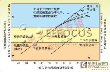
Figure 2: MA2481B universal sensor
As shown in Figure 2, we can see that the diode square law extends from -70dBm to about -20dBm. Common sensors use the square law region formed by the three diode paths to make a true RMS sensor covering a dynamic range from +20dBm to -60dBm. There are two transition points between the diode pairs, the first transition point is about -3.5dBm, and the second transition point is at -23.5dBm.
For the detector A path, there is 40dB of attenuation; this detector is selected if the input power is in the range of +20dBm to -3.5dBm. Therefore, the signal level at the diode varies from -20dBm to -43.5dBm. Detector B has 23dB of attenuation and is selected if the input power range is between -3.5dBm and -23.5dBm. The signal level at the diode varies from -26.5dBm to 46.5dBm.
The last diode-detector pair C has only 6dB of attenuation and is only active when the input level drops below -23.5dBm. The signal level at the diodes varies from -29.5dBm to -66dBm. The system block diagram and physical layout are shown in Figures 3 and 4.
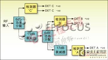
Figure 3: MA2481B universal sensor
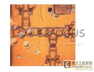
Figure 4: Physical layout of a generic sensor
So what is the advantage of operating with three pairs of diodes? We have a true sensor with an RMS range of 80dB, which is very useful for measuring WCDMA signals generated by UEs, which want to cover a wide dynamic range. Of course, it is possible to make a similar sensor using only two pairs of diode paths. The square law region of the diodes is 50dB, so if we have two paths, each operating over a range of 40dB, this is enough to produce a sensor with a dynamic range of 80dB.
However, let's compare the noise performance of the two sensors. For the two-path sensor, at the mid-switch point of -20dBm, the input power on the diode is equal to -60dBm, and noise at this point will seriously affect the measurement. For the three-path sensor, the lowest signal at any switch point is -46dBm, so the signal-to-noise ratio is much better than with the two-path approach, resulting in faster measurements, but less accurate.
Measurement errors and uncertainties can be divided into four main areas of impact: the power meter, the calibrator, the sensor, and some characteristics of the device under test, such as matching and spurious signal output. We will examine these areas one by one to analyze their contribution to power measurement.
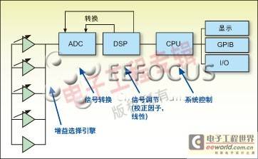
Figure 5: Simplified block diagram of the Anritsu ML2437A power meter.
This is a typical block diagram of a modern power meter. The input signal is amplified, converted to digital, and then processed by a DSP. In traditional power meters, the amplifier is typically set to ten ranges per range. The need for wide dynamic range power sensors has led to the use of analog-to-digital converters with larger dynamic ranges, and each range typically covers a range greater than 10dB.
Anritsu's power meters have five amplifier ranges. The two ranges with the lowest gain are DC coupled and have the advantage of fast response for GSM type applications. The other three ranges are AC amplifiers that are used with a circuit breaker in the sensor. These ranges are used to measure low level signals where stability, noise and drift are the main parameters. If the bandwidth of these ranges is reduced, the noise performance can be improved.
Instrument accuracy
The instrument accuracy of the power meter is less than 0.5%, and can be treated as a general error; this is the performance of the power meter when considered as a baseband voltage measurement system. Some parameters that normally affect this number—such as quantization error and zero carry over—have been greatly reduced by using analog-to-digital converters with higher resolution.
The lowest gain range usually has the largest dynamic range. Let's analyze the effect of quantization on this gain range, as it will be the most important.
On this range, the maximum input voltage to the ADC is 4.5V. The converter is a 16-bit ADC, so the resolution is 68.6uV per bit. The smallest signal that this range must handle is about 80mV, which corresponds to about 1,200 bits of the ADC. Therefore, the quantization error is less than 0.09% and does not need to be treated as a separate item. Other amplifier ranges have smaller dynamic ranges, so the quantization error is much smaller.
Zero Adjustment and Drift
This is a residual effect of the zeroing process and its drift over one hour is measured using the maximum average method. The specification requirement for this parameter is that the error term is less than 0.5% of full scale in the most sensitive range. For the two sensors discussed in this article, the most sensitive range is 10dB.
For fast thermal sensors, the zero adjustment is equal to 0.05mW, while for general-purpose diode sensors, the zero adjustment is equal to 0.05nW. As the power level decreases in the minimum range, the effects of zero adjustment and drift become more important. For signals at the lowest end of the published dynamic range, their contribution is less than 5%.
Calibrator Power Reference
The power reference provides a traceable 0dBm reference level for the power meter to calibrate the sensor. The reference calibration is traceable to national standards and can be considered to have a peak accuracy within +/-1.2% or 0.9% RSS over one year. The other error we want to consider is the mismatch between the sensor to be calibrated and this reference. The reference has a VSWR (voltage standing wave ratio) of less than 1.04, which helps to reduce this error. For the two sensors considered, this error term is 0.31%.
Power Sensors
The power sensor affects the uncertainty budget by five factors:
1. Linearity
The sensor has a linearity specification which is the measured deviation from an ideal power measurement device;
2. Temperature coefficient
Both the thermopile and diode cells have temperature coefficients. Anritsu's sensors are individually corrected for temperature drift and have a small thermistor on the substrate that the power meter uses to calculate the calibration. The calibration is not perfect, so there is still a residual error; typically, this error is less than 1% over a wide temperature range.
3. Mismatch
It is the uncertainty between the sensor and the device under test when making a measurement. This is often the largest factor in the error budget, even if the sensors are well matched.
4. Uncertainty of correction factor
This is a function of the mismatch between the sensor and the calibration system of the correction factor, which is affected by the sensor being measured. So, for example, a 38 GHz fast thermal sensor has a correction factor uncertainty of 3.62%, while a 2.2 GHz generic sensor has a correction factor uncertainty of 0.6%.
5. Noise
This depends on the type of sensor and the applied signal level. For thermopile cells, the noise contribution increases as the signal level decreases. For general purpose sensors, we need to consider the added noise on each set of diodes towards the range transition point. After the range transition, the signal-to-noise ratio improves. The power meter signal channel contributes relatively little to the overall noise performance of the sensor.
Averaging can reduce noise, and the Anritsu ML234X power meter offers several averaging options. At lower powers, there is a facility to automatically increase averaging to maintain fast response at higher power levels.
No match
This is probably the single largest contributor to the error budget when making a measurement. Mismatch error is caused by the impedance mismatch between the sensor and the signal source. In general terms, sensors—which are passive terminations—tend to have better matches than active devices. The reflected wave superimposes the transmitted wave vectorially, creating a standing wave. The sensor will detect this, but it will not be possible to detect the location of the maximum and minimum. Therefore, when considering mismatch error, we always have to assume the worst case scenario.
The equation describing the degree of mismatch is as follows:
![]()
Where s is the signal source and l is the load, in this case the sensor.
Using an attenuator can improve mismatch errors. In Anritsu's power meters, there is a tool that allows the user to enter a table with attenuation values and apply it to the measurement. Precision attenuators can be calibrated to 0.05dB or 1.15%. If a non-precision attenuator is used, the calibration error may be greater than the improvement in mismatch you are looking for.
Harmonics and Spurious Signals
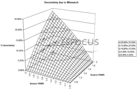
Figure 6: Error surface due to mismatch between signal source and sensor
Another source of error in power measurements is harmonics and spurious signals. A square-law sensor will sum the power of all signals within its passband.
For most completed system designs that meet government or international regulations, the impact of these signals on measurements is negligible. However, for measurements made on incomplete systems or parts of subsystems, these signals can cause additional errors due to the lack of filtering. For example, if a local oscillator leaks through a mixer, the frequency component is only 20dB below the main signal.
The sensor will add the two powers together, which will cause an additional 1% error due to the presence of two signals. If we look at another example, this time the amplifier signal is compressed. In this case, the harmonic output may only be 10dB less than the carrier, so it will add an additional 10% error to the reading, which is large compared to the other errors in the system.
This characteristic of a true RMS sensor is of great advantage during multi-carrier testing. If we take two carriers a few MHz apart, the peak voltage will be 2V. A diode-based peak power meter will then read this as 4x the power, while a true RMS sensor will correctly identify the combined signal as 2x the power.
So, let's look at the effects of these errors on two measurement scenarios. In both cases, we will assume that the signal source has a VSWR of 1.5 and that the spurious output of this signal is negligible.
1. Measure 2.2GHz WCDMA signal at +10dBm using a general purpose sensor.
2. Measure 38GHz RF link using thermal sensor at +10dBm;
In both cases, we assume that noise and zero-drift effects on the measurements are negligible.
The table shows the uncertainties superimposed in the linear and RSS models.
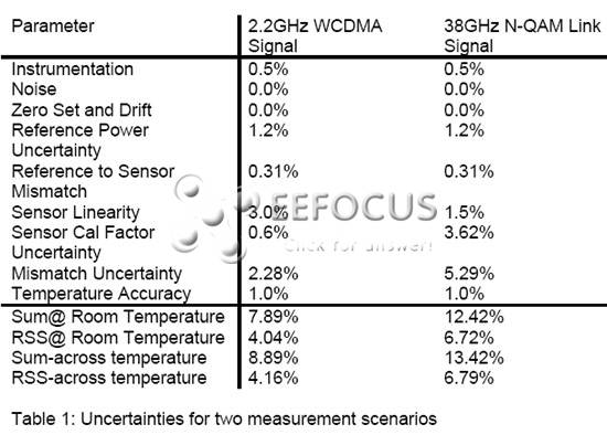
Table 1: Uncertainties for two measurement scenarios
Linear summation assumes that the worst-case errors always add up. RSS summation takes the view that since the errors in the signal sources arise from different physical mechanisms, it is reasonable to assume that they will not add up in the worst-case average.
Many companies and uncertainty schemes have taken this approach when dealing with the sum of uncertainties that are not physically related. If we are to increase our understanding of the uncertainties at these frequencies and power levels, then the best way to do this is to show this in a three-dimensional graphic.

Figure 7: Uncertainty surface for the universal sensor MA2481B, with the worst case already superimposed
For a generic sensor without averaging, this graph shows the sum of the uncertainties at room temperature. The worst case has been added up. The effect of noise on each path of the diode can be seen. With moderate averaging, the noise at the switching point can be reduced to insignificant levels. At low power levels, noise is the largest single factor.
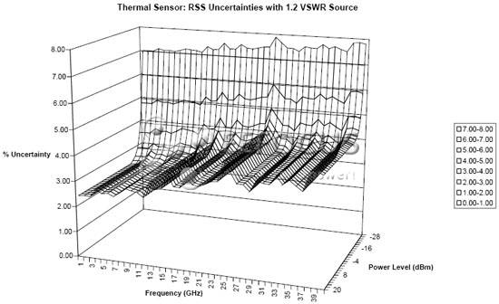
Figure 8: Uncertainty surface of thermal sensor averaged, RSS error added
This figure shows the uncertainty surface of a thermopile sensor over its entire operating frequency range. In this case, the source match has been fixed at 1.2, so the uncertainty due to mismatch has been reduced. The uncertainty has been superimposed as an RSS term. The increase in uncertainty at low power levels is mainly caused by the zero adjustment parameter. This frequency-dependent ripple is caused by the uncertainty of the correction factor that varies over the entire range.
The 2.5% uncertainty, which is the lowest uncertainty on the graph, is just over +/-0.1dB, while the 8% uncertainty, which is the largest uncertainty on the graph, is +0.33/-0.36dB.
Conclusion
With the right sensor technology, accurate true RMS measurements can be made on signals with complex modulation. This article describes the various factors that need to be considered when calculating the uncertainty budget when measuring power.
At large signal power levels, the most important single effect is mismatch, which can be managed using matching techniques such as precision attenuators; at low power levels, the most important effect is noise, which can be managed by choosing appropriate averaging conditions on the power meter.
Previous article:Get the best distortion level with the Gain Test Tip
Next article:A "Test-by-Design" Approach to Low-Power Devices
- Keysight Technologies Helps Samsung Electronics Successfully Validate FiRa® 2.0 Safe Distance Measurement Test Case
- From probes to power supplies, Tektronix is leading the way in comprehensive innovation in power electronics testing
- Seizing the Opportunities in the Chinese Application Market: NI's Challenges and Answers
- Tektronix Launches Breakthrough Power Measurement Tools to Accelerate Innovation as Global Electrification Accelerates
- Not all oscilloscopes are created equal: Why ADCs and low noise floor matter
- Enable TekHSI high-speed interface function to accelerate the remote transmission of waveform data
- How to measure the quality of soft start thyristor
- How to use a multimeter to judge whether a soft starter is good or bad
- What are the advantages and disadvantages of non-contact temperature sensors?
- Innolux's intelligent steer-by-wire solution makes cars smarter and safer
- 8051 MCU - Parity Check
- How to efficiently balance the sensitivity of tactile sensing interfaces
- What should I do if the servo motor shakes? What causes the servo motor to shake quickly?
- 【Brushless Motor】Analysis of three-phase BLDC motor and sharing of two popular development boards
- Midea Industrial Technology's subsidiaries Clou Electronics and Hekang New Energy jointly appeared at the Munich Battery Energy Storage Exhibition and Solar Energy Exhibition
- Guoxin Sichen | Application of ferroelectric memory PB85RS2MC in power battery management, with a capacity of 2M
- Analysis of common faults of frequency converter
- In a head-on competition with Qualcomm, what kind of cockpit products has Intel come up with?
- Dalian Rongke's all-vanadium liquid flow battery energy storage equipment industrialization project has entered the sprint stage before production
- Allegro MicroSystems Introduces Advanced Magnetic and Inductive Position Sensing Solutions at Electronica 2024
- Car key in the left hand, liveness detection radar in the right hand, UWB is imperative for cars!
- After a decade of rapid development, domestic CIS has entered the market
- Aegis Dagger Battery + Thor EM-i Super Hybrid, Geely New Energy has thrown out two "king bombs"
- A brief discussion on functional safety - fault, error, and failure
- In the smart car 2.0 cycle, these core industry chains are facing major opportunities!
- Rambus Launches Industry's First HBM 4 Controller IP: What Are the Technical Details Behind It?
- The United States and Japan are developing new batteries. CATL faces challenges? How should China's new energy battery industry respond?
- Murata launches high-precision 6-axis inertial sensor for automobiles
- Ford patents pre-charge alarm to help save costs and respond to emergencies
- What are the advantages of PHY6212 that can support Bluetooth Mesh networking (I)
- Problems with CD4051
- 【Smart Access Control System】
- USB to TTL module USB driver for the Corelinks SinA33 development board
- Application of millimeter wave radar technology in corner radar
- Do you know how to benefit from a better way to power your devices? Talk to Vicor engineers!
- UV Sterilization Box TI Solution
- Not just nostalgia - a complete collection of radio principles, circuits, repairs and assembly information
- Interface and Programming of Serial A/D Converter TLC2543 and 80C196
- WeChat Mini Program IoT Solution

 Infrared optical communication
 Introduction to the LTC2996 High Accuracy Temperature Monitor


 京公网安备 11010802033920号