Ultrasonic electronic guide circuit
Source: InternetPublisher:D先生 Keywords: ultrasound Updated: 2024/06/20
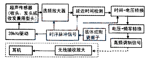
This design is to install electronic devices on the soles of the feet of blind people or people with low vision, use ultrasonic sensors to accurately measure the distance between the center of the forefoot of the sole and the ground, convert the distance into time, and then convert the time into voltage. The voltage-controlled oscillator generates audio oscillations, and its frequency is related to the distance. Then it is transmitted wirelessly to the receiving electronic device on the head of the blind person to drive the headphones. The two shoes share a channel because both feet cannot leave the ground at the same time when walking, and only one left/right channel works. When one foot is lifted, the sensor on the sole detects that the sound frequency is generated when it is greater than 10 cm. The greater the distance, the higher the tone (frequency). When walking on flat ground, the tone changes smoothly. When going down the stairs, lift your foot and take a step forward - fall down, and you can normally hear a large change in the tone. When encountering a deep pit greater than 30cm, the tone will be very sharp, which serves as a prompt. Its principle block diagram is shown in the figure below.
1. Generation of timing signals
Because it is powered by batteries, the voltage will gradually decrease with the use time.
The frequency of the usual RC oscillator is unstable. The 465kHz ceramic resonator of the usual radio is used to generate oscillation, and then after 12 frequency division, a 39kHz signal is obtained. After a series of frequency divisions, various required timing pulse signals can be obtained. There is only one CMOS inverter inside the 4069, generally called a non-buffered gate, represented by "UB", which is suitable for a crystal oscillator from 32KHz to 465kHz. The negative feedback of R2 in the figure below makes the UID work in the linear amplification area, which is about 1/2 of the power supply voltage. There is a slight change at the 9th pin of UID. After the two-stage inversion of UID and UIE, a signal of amplification r with the same phase is obtained. After the X2 three-terminal ceramic filter, only the 465kHz signal can pass through and positively feedback to the 9th pin of UID. Continuous oscillation is formed. At this time, if R2 is removed, there will still be oscillation. Without R2, when the power is just turned on, the UID pin 9 may have only a few tenths of a volt, the pin 8 output is high, and the UIE pin 11 is low.
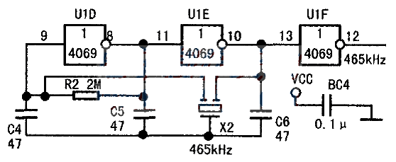
In the switching state, it cannot amplify small signals. It does not oscillate. Occasionally touching the 9th pin may start working, but it may not be stable. It can be seen that the role of R2 is to pull the level of the 9th pin of the UID to the linear region. If 74HC04 replaces 4069, because each gate inside the 74HC04 has three stages of inverting gates, after connecting R2, an odd-level ring oscillator structure has been formed, and even without X2, there are already several megahertz oscillations. Connecting X2 is also difficult to achieve the purpose. C4, C5, and C6 are matching capacitors. The frequency can also be fine-tuned. The actual frequency after connection is 470kHz.
U2 is a D flip-flop. When the clock goes from low to high, the state of Q is equal to D. If Q and D are connected, it becomes a divider-by-two, and the clock flips once each time. At the beginning, Q=0O, Q=1, D=Q is equal to 1. When the clock comes once, Q becomes 1, Q=0, D=Q is equal to 0, and it is ready for the next clock to become 0. The clock changes twice and Q changes once, which is a divider-by-two. Connecting two stages of D flip-flops in series, it becomes a divider-by-four. Now to divide by three, we need to add some feedback. The simple method is shown in the figure below. U2A is a divider-by-two, and its output, Q1 sends the clock of U2B, Q1 becomes O, Q1 becomes 1, and Q2 flips. When there is no feedback, the state of Q2Q1 is 00, 01, 10, 11. When the state 11 is immediately cleared to 0, both inputs of the NAND gate U3D are 1, the output is 0, U3C outputs 1, and the D flip-flop is cleared to 0.
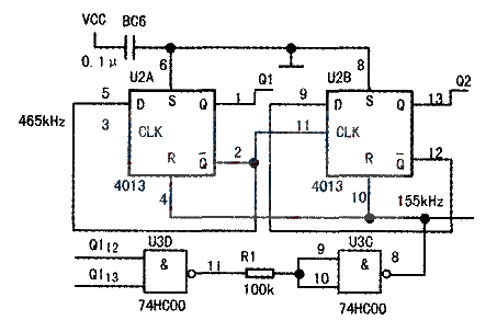
The role of R1 is to delay and widen the clear pulse to 300ns. 1/3 of the signal can be output from U3C, and Q2 can also be used, but Q1 cannot be used.
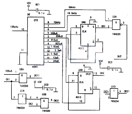
The 155kHz signal is sent to the 10th clock terminal of U6 of the 12-stage binary asynchronous counter 4040. The asynchronous counter is equivalent to 12 D flip-flops connected in series with a frequency division by two. The next stage can only flip when the previous stage changes from 1 to 0. Each stage has a transmission delay of 500ns, and it accumulates step by step. The figure below is the waveform of each stage. Obviously, the signal with a period of 206us changes from 1 to 0 first, and the signal with a period of 3.3ms delays about 3μs from 0 to l, triggering U4A and U4B to flip and output 1.
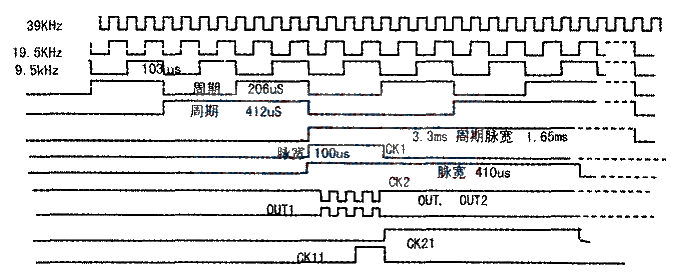
During the negative pulse of the signal with a period of 206μs, the time is equal to 103μs-3μs, and the output CK1 of U4A maintains 1. During the positive pulse of the signal of 206μs, the signal is connected to the R end of the 4th pin of U4A, and CK1 is cleared to 0. This state has to wait for 3.3ms until the periodic trigger signal comes again, and then it will repeat once. The pulse width of CK1 is 100μs and the period is 3.3ms.
Similarly, the pulse width of CK2 can be analyzed as 410μs and the period is 3.3ms. Because of the polarity problem of the clear signal, the 4013 in the figure below cannot be replaced by 74HC74.
The 39kHz signal output from the 7th pin of 4040 and CK1 are combined into an OUT signal containing 4 pulses through U3A and sent to the driver stage. CK1 and 103}Ls are combined into CK11 through U3A, which is a signal with a period of 3.3ms when the second half of the positive pulse of CK1 is high. CK21 is a signal with a period of 3.3ms when the second half of the positive pulse of CK2 is high. These signals will be useful later.
2. Transmitter drive circuit
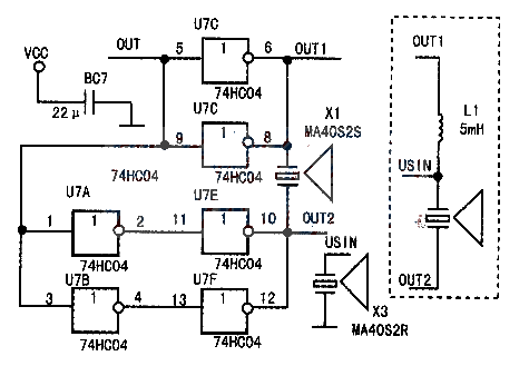
Because the input capacitance of the ultrasonic sensor is as much as 2700pF, the effect of using a single CMOS inverting gate to drive it is poor under low voltage. Now, two parallel push-pull drives are used (as shown in the figure below). The circuit in the virtual box is the circuit using the transceiver head L1. When transmitting, L1 and the sensor are in series resonance to enhance the transmission; when receiving, the fixed level of OUT1 and OUT2 is equivalent to AC grounding, and L1 and the sensor are in parallel resonance to enhance the receiving signal. Theoretically, it is very good, but the actual test effect is very poor. Therefore, the subsequent tests are done with two transceiver heads. The two heads are installed in parallel, with a distance of 2.5cm, and the outlet is at least 1cm from the ground. Since the ultrasonic wave is 8.5mm long, a 0.5mm thick metal protective strip in front of the outlet will not affect the effect.
Because the input capacitance of the ultrasonic sensor is as much as 2700pF, the effect of using a single CMOS inverting gate to drive it is poor under low voltage. Now, two parallel push-pull drives are used (as shown in the figure below). The circuit in the virtual box is the circuit using the transceiver head L1. When transmitting, L1 and the sensor are in series resonance to enhance the transmission; when receiving, the fixed level of OUT1 and OUT2 is equivalent to AC grounding, and L1 and the sensor are in parallel resonance to enhance the receiving signal. Theoretically, it is very good, but the actual test effect is very poor. Therefore, the subsequent tests are done with two transceiver heads. The two heads are installed in parallel, with a distance of 2.5cm, and the outlet is at least 1cm from the ground. Since the ultrasonic wave is 8.5mm long, a 0.5mm thick metal protective strip in front of the outlet will not affect the effect.
3.
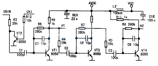
The calculation and design of the three-stage 5-fold bandpass filter in the receiving amplifier circuit are similar to those in the previous issue, but here transistors are used instead of operational amplifiers. The principle is the same, which can save more power and be smaller in size. The signal enters from USIN. When CKl:1, during the transmission, VT2 short-circuits the signal to prevent strong signals from entering the amplifier. The amplified signal is output from Hl and H2.
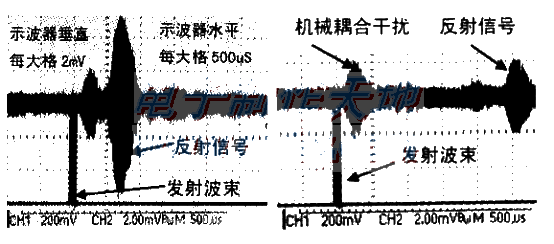
Because they are installed on the same printed circuit board, there is mechanical coupling. As can be seen from the middle and lower figures, there is a fixed receiving peak (mechanical coupling) at 300μs after the transmission signal. This signal is smaller than the reflected wave signal at a distance of 7cm from the ground, and is similar in size to the reflected wave signal at a distance of 20 to 30cm. Moreover, the background noise frequency is 39kHz and the amplitude is about 1mV. Detection is somewhat difficult. We divide the detection into two sections according to the signal strength Hl and H2, and analyze them according to the delay time (distance): ① In the case of 7cm from the ground, the input signal is particularly large, and it has exceeded 200mV (Vpp) after the first stage of amplification. At this time, the signal is sent from Hl to the first detector. When the detector detects a signal, DETOUT2=1. At this time, the second detector may also receive the signal (the signal is half on both sides at 410us). It may also not receive the signal. ② 7cm~30cm from the ground, the received signal gradually decreases from large to large as the distance increases from near to far, and is finally drowned by the 1mV (Vpp) background noise. At the same time, the signal delay is 125 times from 410μ to 33mS, and the amplifier amplifies the noise to 125mV. When the signal is above 250mV, it is detected by the first detector, and DETOUT1=1. At this time, DETOUT2: 0, DETOUT1=1 or 0 (farther away) ③ 30cm~50cm from the ground, the signal cannot be detected, DETOUT2=DETOUT1=0. In the first case, silence is required; in the second case, a tone change is required; if it cannot be received, it is the same as ③; in the third case, a warning tone is required. In the figure, C16, L1, and BC9 are used for power supply filtering.
4. Detection amplifier circuit
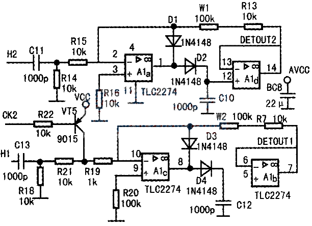
The general diode detector has loss due to the forward voltage drop of the diode, especially in the case of small signals. The figure below uses the high gain of the operational amplifier to offset the forward voltage drop loss of the diode to achieve ideal detection. The
negative half cycle of H2 is amplified by Ala inversion to become a large positive signal, which reaches the positive polarity input terminal of Alb through D4. C12 is charged to the peak value, and Alb is connected to a follower circuit. The signal at pin 7 is always consistent with that at pin 5. R17 and W2 are connected in series and negatively fed back to pin 10 of A1c. At this time, D3 does not work due to reverse bias. Ala inversion amplification is limited. According to the assumptions of "virtual open" and "virtual short" of the operational amplifier, at the peak, the sum of the current fed back from pin 14 to pin 2 through R17+W2 and the current of H2 through R15 is zero. UH2/R15+U14/(R17+W2)=0,U14/UH2=-(R17+W2)/R15=-1~-10 times. When H2 is in the negative half cycle but less than the peak value, the absolute value of the feedback current exceeds the input current, pulls pin 2 high, pin 1 becomes low, and D3 turns on to absorb the feedback current. Maintain the same voltage between pins 2 and 3. (Virtual short) When it is in the positive half cycle, the Ala inverting amplifier output 1 is low, D4 is not connected, and D3 turns on to absorb the positive half cycle current. The detection gain can be controlled by adjusting the potentiometer.
During CK2=0, VT5 turns on, the detection input terminal is pulled high, and the output DETOUT1=0. In order to output full amplitude, the so-called "rail-to-rail"
CMOS op amp is used here, and LM324 is not suitable. The TLC2274 is commonly available in SOD packaging. During the test, a replacement seat is made to convert it into DIP for easy plugging and unplugging.
5. The distance-pulse-digital conversion
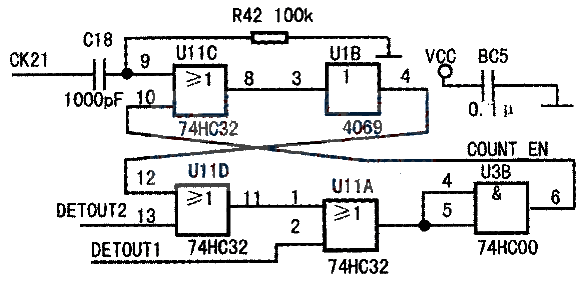
circuit is shown in the figure above. CK21 is an S signal. The positive pulse rise time of CK21 passes through U11C=1, UIB=0, U1D=OU3B=1 (referring to the output end), COUNT_EN=1 (start counting) and returns to the input end of U11C to complete the setting process of an RS trigger. Although the CK21 overshoot disappears, the set state still exists. DETECT2 is an R signal, DETECT2=1, U11D=1, U3B=0, U11C=0, UIB=1; reset state, COUNT_EN=0 (stop counting). DETECT1 is the priority reset signal. Regardless of whether CK21 has an overshoot or not, as long as DETECT1=1, COUNT_EN=0.
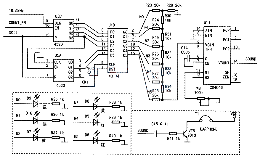
In the figure below, U5-4520 is a dual hexadecimal counter. COUNT_EN controls the counting gate. The pulse width of COUNT_EN contains as many 19.5KHz as it counts. This number is latched in U10-40174 at the rising time of CK1. Then CK11 comes and clears the counter to prepare for the next count. There is a 50uS time interval between the rising time of CK1 and CK11. U5B and U5A are cascaded, and U5B-Q3 should be connected to U5A-EN, that is, using the falling edge count, U5B-Q3 from 1 to 0, the higher bit count is increased by 1. CP cannot be used. In the test phase, D5~ Dl0 is temporarily connected to detect the state of N5~ NO. This is a typical 6-bit binary number, N5~ NO= 000000~111111, indicating that the distance is from near to far.
6. Digital-voltage-tone conversion circuit.
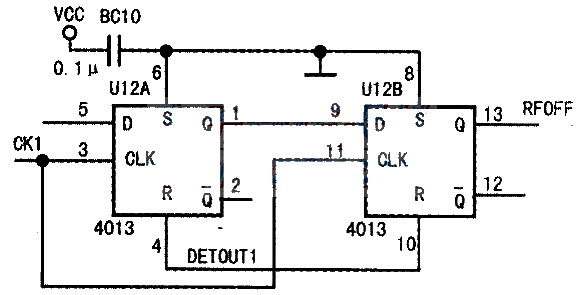
In the figure below, R23~R34 constitute an R-2R ladder D/A conversion circuit. The principle is described in the textbook and will not be repeated here. The resistor should be a 5-circle color ring, with the last circle being brown (1%). It is best to use a digital multimeter to measure it and select a resistance close to the nominal value. N5~N0= 000000, corresponding to an output voltage of 0, N5~N0: 111111, corresponding to an output voltage VCC multiplied by 63/64. There are 64 different levels in total. Because there will be no detection signal during the CK2 pulse width of 410uS, the actual 0.8 data does not exist. 4046 is a phase-locked loop, and its main uses are: digital frequency synthesis, phase discrimination, VF conversion, etc. We only use its VF conversion function. The DC level is added to the input terminal 9 of the voltage-controlled oscillator of U11-4046. The higher the voltage, the higher the oscillation frequency. The frequency can be adjusted by selecting appropriate C14 and adjusting W3. The resistor and capacitor affect the slope of the VF characteristic curve. The highest frequency is the input Vcc condition, adjusted to FMax=5KHZ. When the input is 9/64Vcc, the tone drops to 100HZ or lower. In order to hear a higher tone at the lower end, connect a 100K-500K resistor to the 12th foot of U11 and adjust it to Fmin=100HZ. The connection of this resistor affects the VF characteristic curve to move upward by a fixed value. During the experiment, you can listen to it with VT6 and headphones. After the experiment, connect SOUND to the wireless transmission module. In order to transmit alternately with both feet, when a foot touches the ground, the DETOUT1 of the foot is 1, and U12A and B are cleared, as shown in the right figure. Regardless of whether CK1 is coming or not, RFOFF is always 0, turning off the wireless transmission module of the foot. Lift your foot, DETOUT1=0, CK1 comes twice, and the D flip-flop sends Vcc from the D of pin 5 to the Q of pin 1, and then to the Q of pin 13, making RFOFF high and starting the wireless transmission module of that foot. Since both feet cannot leave the ground at the same time when walking, only the lifted foot can transmit, achieving the purpose of guiding the blind with both feet in turn.
In the figure below, R23~R34 constitute an R-2R ladder D/A conversion circuit. The principle is described in the textbook and will not be repeated here. The resistor should be a 5-circle color ring, with the last circle being brown (1%). It is best to use a digital multimeter to measure it and select a resistance close to the nominal value. N5~N0= 000000, corresponding to an output voltage of 0, N5~N0: 111111, corresponding to an output voltage VCC multiplied by 63/64. There are 64 different levels in total. Because there will be no detection signal during the CK2 pulse width of 410uS, the actual 0.8 data does not exist. 4046 is a phase-locked loop, and its main uses are: digital frequency synthesis, phase discrimination, VF conversion, etc. We only use its VF conversion function. The DC level is added to the input terminal 9 of the voltage-controlled oscillator of U11-4046. The higher the voltage, the higher the oscillation frequency. The frequency can be adjusted by selecting appropriate C14 and adjusting W3. The resistor and capacitor affect the slope of the VF characteristic curve. The highest frequency is the input Vcc condition, adjusted to FMax=5KHZ. When the input is 9/64Vcc, the tone drops to 100HZ or lower. In order to hear a higher tone at the lower end, connect a 100K-500K resistor to the 12th foot of U11 and adjust it to Fmin=100HZ. The connection of this resistor affects the VF characteristic curve to move upward by a fixed value. During the experiment, you can listen to it with VT6 and headphones. After the experiment, connect SOUND to the wireless transmission module. In order to transmit alternately with both feet, when a foot touches the ground, the DETOUT1 of the foot is 1, and U12A and B are cleared, as shown in the right figure. Regardless of whether CK1 is coming or not, RFOFF is always 0, turning off the wireless transmission module of the foot. Lift your foot, DETOUT1=0, CK1 comes twice, and the D flip-flop sends Vcc from the D of pin 5 to the Q of pin 1, and then to the Q of pin 13, making RFOFF high and starting the wireless transmission module of that foot. Since both feet cannot leave the ground at the same time when walking, only the lifted foot can transmit, achieving the purpose of guiding the blind with both feet in turn.
When designing, pay attention to connecting a bypass capacitor BCn between the power supply and ground of each digital circuit. It seems that it is not very useful. In fact, it is very important to improve reliability. Because all signals change at the moment of certain clock jumps, the NMOS tube and PMOS tube inside the CMOS circuit are turned on, and the jump of the level needs to charge and discharge the load. At this moment, the power supply current is suddenly very large, and the distributed inductance of the printed circuit board leads hinders the sudden change of current. The power supply voltage drops instantly. If at this time, all the high-level output pins of this circuit have a sharp burr that jumps down. Similarly, the distributed inductance of the ground wire leads causes all low-level output pins to have a sharp burr that jumps up. In order to prevent this from happening, the bypass capacitor BCn is connected between the VDD and GND of the circuit. Since the voltage of the capacitor cannot jump, the occurrence of burrs is greatly reduced. Of course, this capacitor cannot be too far away from the protected circuit.
Latest Other Circuits
- Frequency signal tracking circuit (phase-locked loop circuit) composed of CD4046
- Using VPX-based PCIe systems for asynchronous clocking
- Bookcase moth-proofing circuit made with 7556 dual-time base circuit
- How to Design a Wireless Remote Controlled Two-Wheeled Robotic Rover Using ESP8266 and Arduino Uno
- How to Control Large Linear Actuators with Arduino
- DIY an electronic card lock security system
- Semi-automatic flame cutting machine electrical control circuit
- bridge stabilizing link circuit
- Water level automatic controller circuit
- Z32A, Z32K, Z3025J radial drilling machine electrical schematic circuit
Popular Circuits
- Ultrasonic receiver circuit diagram for echo detection distance
- Ultrasonic blind pathfinder circuit
- R-40-16 ultrasonic receiving circuit
- Ultrasonic remote control switch circuit
- SC41342 (general) infrared, ultrasonic or radio frequency remote control transmission encoding circuit-02
- MC145026 (cordless phone and half-duplex remote control) infrared, ultrasonic or radio frequency remote control encoding circuit
- Circuit for measuring distance using ultrasonic waves 03
- Ultrasonic resonance circuit
- Ultrasonic multifunctional electric fan remote control circuit
- SY-1001 ultrasonic remote control switch


 京公网安备 11010802033920号