Series switching power supply output voltage filter circuit
Source: InternetPublisher:念念Brown Keywords: switching power supply power switching voltage regulator Updated: 2020/08/01
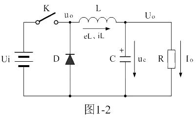
The output of most switching power supplies is DC voltage. Therefore, the output circuit of the switching power supply generally has a rectifier and filter circuit. Figure 1-2 is a working principle diagram of a series switching power supply with rectification and filtering functions.

Transfer files for PCB proofing
Figure 1-2 is based on the circuit of Figure 1-1-a, adding a rectifier diode and an LC filter circuit. Among them, L is the energy storage filter inductor. Its function is to limit the large current Ton when the control switch K is turned on, preventing the input voltage Ui from being directly added to the load R, causing a voltage impact on the load R, and at the same time reducing the current iL flowing through the inductor. Convert it into magnetic energy for energy storage, and then when the control switch K is turned off, Toff converts the magnetic energy into a current iL to continue to provide energy output to the load R; Part of the current flowing through the energy storage inductor L is converted into charges for storage, and then during the turn-off period of the control switch K, Toff converts the charges into current to continue to provide energy output to the load R; D is the rectifier diode, whose main function is freewheeling, so It is called a freewheeling diode, and its function is to provide a current path for the energy storage filter inductor L to release energy during the turn-off period of the control switch Toff.
During the turn-off period of the control switch Toff, the energy storage inductor L will generate a counter electromotive force. The current iL flowing through the energy storage inductor L flows out from the anode of the counter electromotive force eL, passes through the load R, and then passes through the anode of the freewheeling diode D, and then flows from the positive electrode of the back electromotive force eL. The negative electrode of the current diode D flows out, and finally returns to the negative electrode of the back electromotive force eL.
For Figure 1-2, if you ignore the control switch K and the input voltage Ui, it is a typical inverse г filter circuit. Its function is to smooth the pulsating DC voltage and output its average value.
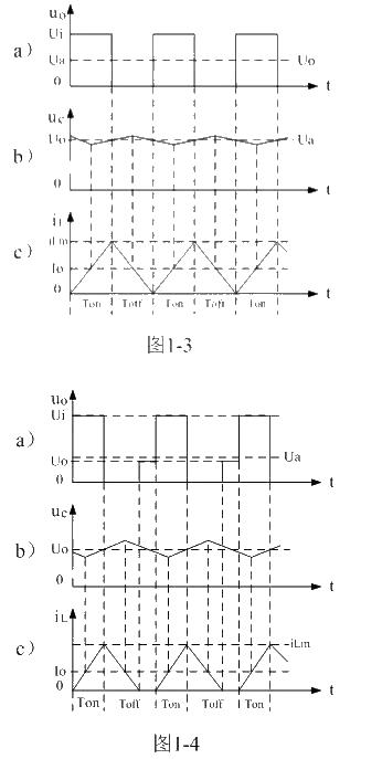
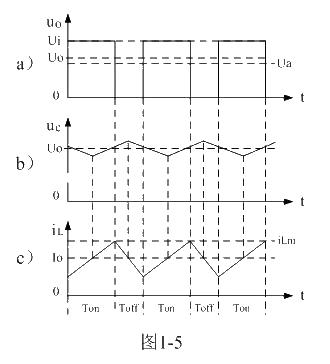
Figure 1-3, Figure 1-4, and Figure 1-5 are the voltage and current waveforms of several key points in the circuit of Figure 1-2 when the duty cycle D of the control switch K is equal to 0.5 and 0.5 respectively. Figure 1-3-a), Figure 1-4-a), Figure 1-5-a) are the waveforms of the output voltage uo of the control switch K respectively; Figure 1-3-b), Figure 1-4-b), Figure 1-5-b) respectively shows the waveform of the voltage uc across the energy storage filter capacitor; Figure 1-3-c), Figure 1-4-c) and Figure 1-5-c) respectively show the waveforms flowing through the energy storage inductor. The waveform of L current iL.

Transfer files for PCB proofing

Transfer files for PCB proofing
During Ton, the control switch K is turned on, and the input voltage Ui outputs the voltage uo through the control switch K, and then is added to the filter circuit composed of the energy storage filter inductor L and the energy storage filter capacitor C. During this period, the energy storage filter inductor L The voltage eL at the terminal is:
eL = Ldi/dt = Ui – Uo —— K on-time period (1-4)
In the formula: Ui input voltage, Uo is the DC output voltage, that is: the average value of the voltage uc across the capacitor.
By the way, here is a note: Since the voltage change ΔU across the capacitor is very small relative to the output voltage Uo, for simplicity, we treat Uo as a constant here. In some cases, if it is necessary to analyze the initial charging and discharging process of a capacitor, a differential equation must be established and solved. Because it takes a certain amount of time to establish the output voltage Uo, the results obtained by accurate calculation are generally
All contain exponential function terms. When the time variable is equal to infinity, that is, when the circuit enters a steady state, and then the relevant parameters are averaged, the result is basically equal to (1-4).
Integrating equation (1-4) gives:

Transfer files for PCB proofing
In the formula, i(0) is the switching moment of control switch K (time t = 0), that is, the current flowing through the inductor L at the moment when the control switch K is turned on, or the initial current flowing through the inductor L.
When the control switch K suddenly switches from the on period Ton to the off period Toff, the current iL flowing through the inductor L reaches the maximum value:
iLm =(Ui-Uo)Ton/L + i(0) —— Moment before K turns off (1-6)
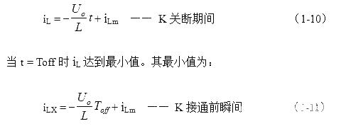
During Toff, the control switch K is turned off, and the energy storage inductor L converts the magnetic energy into a current iL, and continues to provide energy to the load R through the rectifier diode D. During this period, the voltage eL across the energy storage filter inductor L is:
eL = Ldi/dt = – Uo —— K turn-off period (1-7)
In the formula, the negative sign before –Uo means that the direction of the electromotive force generated by the inductor during K is turned off is exactly opposite to the direction of the electromotive force generated by the inductor during K is turned on. Integrating equation (1-7) gives:

Transfer files for PCB proofing
In the formula, i(Ton+) is the current flowing through the inductor before the moment when the control switch K switches from Ton to Toff. i(Ton+) can also be written as i(Toff-), that is: the moment when the control switch K turns off or on, The current flowing through the inductor L before and after is equal. In fact, i(Ton+) in equation (1-8) is iLm in equation (1-6), that is:

Transfer files for PCB proofing
The above calculations are all based on the assumption that the output voltage Uo is basically unchanged. This is exactly the case in practical application circuits. The voltage ripple of the output voltage Uo is very small, only a few percent of the output voltage. In engineering calculations, it is completely Can be ignored.
It can be seen from equation (1-4) to (1-11) and Figure 1-3, Figure 1-4, and Figure 1-5:
When the switching power supply operates in critical continuous current or continuous current state, during the entire period when K is on and off, the energy storage inductor L has current flowing out, but during the period when K is on and K is off, the current flows through the storage inductor L. The rate of rise (absolute value) of the current in the inductor L is generally different. During the period when K is on, the rising rate of the current flowing through the energy storage inductor L is Ui-Uo/L:; During the off period of K, the rising rate of the current flowing through the energy storage inductor L is: -Uo/L
therefore:
(1) When Ui = 2Uo, that is, when the filtered output voltage Uo is equal to half of the power supply input voltage Ui, or when the duty cycle D of the control switch K is half, the rise rate of the current flowing through the energy storage inductor L, During the period when K is on and when K is off, the absolute values are exactly the same, that is, the speed at which the inductor stores energy is exactly the same as the speed at which it releases energy. At this time, i(0) in equation (1-5) and iLX in equation (1-11) are both equal to 0. In this case, the current iL flowing through the energy storage inductor L is the critical continuous current, and the filtered output voltage Uo is equal to the average value Ua of the filtered input voltage uo. See Figure 1-3.
(2) When Ui > 2Uo, that is: when the filtered output voltage Uo is less than half of the power input voltage Ui, or when the duty cycle of the control switch K is less than half: Although during the period when K is turned on, the stored energy flows through The current rise rate (absolute value) of the inductor L is greater than the current rise rate (absolute value) flowing through the energy storage inductor L during the K turn-off period; but since i(0) in (1-5) is equal to 0, And Ton is smaller than Toff. At this time, iLX in (1-11) will have a negative value, that is, the output voltage will in turn charge the inductor, but due to the existence of the rectifier diode D, this is impossible, which means that the flow The current of the energy storage inductor L crosses 0 early, that is, there is a current interruption. In this case, the current iL flowing through the energy storage inductor L is not a continuous current, and the switching power supply operates in a discontinuous current state. Therefore, the ripple of the output voltage Uo is relatively large, and the filtered output voltage Uo is smaller than the filtered input voltage uo. Average Ua. See Figure 1-4.
(3) When Ui < 2Uo, that is: when the filtered output voltage Uo is greater than half of the power input voltage Ui, or when the duty cycle of the control switch K is greater than half: During the period when K is turned on, although the stored energy flows through The current rise rate (absolute value) of the inductor L is less than the current rise rate (absolute value) of the current flowing through the energy storage inductor L during the K turn-off period. However, since Ton is greater than Toff, i(0) in (1-5) and iLX in (1-11) are both greater than 0, that is, the energy stored in the inductor cannot be fully released every time. In this case, the current iL flowing through the energy storage inductor L is a continuous current, the switching power supply works in a continuous current state, the ripple of the output voltage Uo is relatively small, and the filtered output voltage Uo is greater than the average value Ua of the filtered input voltage uo . See Figure 1-5.
- How much current can a 2N3055 solar cell produce? How can I get 3055V from a 12N2 solar cell?
- Driving circuit of switching power supply field effect tube
- Basic circuit description of adjustable voltage regulator LM317
- INA155/INA156 is used to form a single-supply high-side current monitor for detecting load current
- Low cost and high performance LED constant current power supply
- Electric bicycle battery charger circuit
- Car Audio Power Supply
- LM317T voltage regulation adjustable circuit diagram explanation
- Battery powered switching circuit diagram
- Solar Lead Acid Battery Charger
- Which one is more suitable: linear power supply, thyristor power supply or switching power supply?
- Some techniques for measuring inductor current
- Layout and design principles of switching power supply
- Self-switching power supply
- Switching power supply high withstand voltage constant current source circuit diagram
- Parallel switching power supply for televisions (c)
- Switching power supply drive circuit
- Application of TDK high-power field effect tube full-bridge components in switching power supplies and class D amplifiers 01
- High-fidelity power amplifier using switching power supply 02
- Switching power supply starting circuit diagram using field effect transistor


 京公网安备 11010802033920号