|
An interesting thing happened while writing the “ Six Ways to Keep Capacitive Loads Stable ” section. We selected a CMOS op amp with a “rail-to-rail” output and measured R OUT , but there was no loop gain in the high frequency region, so we could not determine R O . Based on the R O measurement, we predicted the location of the second pole in the amplifier’s “ corrected Aol plot” with a 1μF capacitive load . To our great surprise, the Tina SPICE simulation was off when the “ corrected Aol ” plot was processed by x5 ! Based on the previous first-round analysis results, this error was well beyond the acceptable limit, so we took a closer look at the amplifier output impedance.
This seventh part of the series focuses on the amplifier's open-loop output impedance, Z O , for the two most common output topologies used for small-signal amplifiers . For a traditional bipolar emitter -follower , the amplifier output stage, Z O , is well behaved and primarily resistive (R O ) across the unity-gain bandwidth of the amplifier . However, for many CMOS rail-to-rail output amplifiers, Z O is both capacitive and resistive across the unity-gain bandwidth of the amplifier .
This article does not analyze the bipolar topology of "all NPN outputs", which is most commonly used in power operational amplifiers , an amplifier that can provide currents from 50mA to over 10A and operates in the linear region . Having a good knowledge of output impedance is very important and will help to correctly predict the " corrected Aol plot " and is also a basic tool in network synthesis techniques for stabilizing amplifier circuits.
Bipolar emitter follower output amplifier Z O
Figure 7.1 shows a typical bipolar output stage for an emitter follower topology. In this type of output stage, R O (small signal, open loop output resistance) is usually the dominant component of Z O (small signal, open loop output impedance). For a given DC current load, R O is generally constant. We will first analyze some rules of thumb for emitter follower R O and then use these rules to predict R O for different values of DC output current . Finally, we will use the Tina SPICE simulation program to verify that the predicted values are correct.
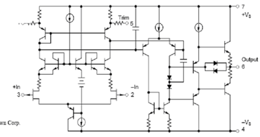
Figure 7.1: Key parameters of the OPA542 -Typical emitter follower, bipolar output amplifier
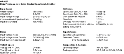
Figure 7.2 shows the parameters of a typical emitter follower, bipolar output amplifier. When the input bias current is in the nA range (such as 10nA ), devices using this topology can achieve excellent characteristics such as extremely low noise and offset input parameters. Some bipolar amplifiers use JFETs in the input stage to reduce the input bias current to very low pA levels. The input stage range of this common mode is generally around 2V for both supplies. The output voltage swing is usually limited to within 2V of either power rail or slightly higher. Amplifiers using dual supplies (such as +/-5V to +/-15V ) generally achieve the best performance. Figure 7.2: Example parameters : emitter follower, bipolar output amplifier
A simplified model of an advanced emitter-follower, bipolar amplifier employs two GM ( current gain ) stages followed by a transistor voltage follower output stage as shown in Figure 7.3 . The open-loop output impedance, Z O , is determined primarily by R O and is constant for the unity-gain bandwidth of the amplifier.
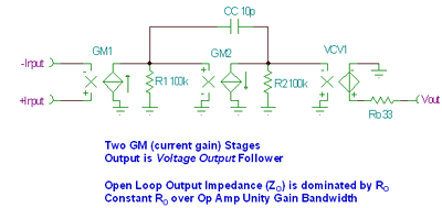
Figure 7.3: Two-stage simplified model : emitter follower, bipolar output amplifier
For most amplifiers , the class AB bias current of the output stage is approximately of the total amplifier quiescent current when the amplifier output is unloaded . The R O of a bipolar transistor is proportional to 1/gm, where gm is the transistor's current transfer ratio or current gain. Since gm is proportional to the collector current, IC, R O is inversely proportional to IC. As IC increases from no - load output current to full - load output current , R O decreases . This might lead one to assume that R O would be zero at a certain input current limit . However, this assumption is not true due to transistor physics, internal drive, and bias arrangement . We will measure the value of R O at the highest available load current and define it as R X . We will then measure the value of R O at no -load current and derive a constant, K Z , for a given amplifier circuit that can be used to predict the behavior of R O at any load current. From Figure 7.4 , we can clearly see how the output term of the emitter follower can be used to describe the path from the front-end gm stage to the amplifier output pin.
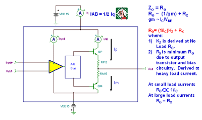
Figure 7.4: Z O Definition : Emitter Follower, Bipolar Output Amplifier
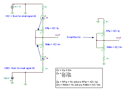
Figure 7.5 details the emitter follower Z O model with constant R X , measured at full load current, with a series current control resistor and transfer function K Z / I C. Since the device has push ( PNP transistor) and pull ( NPN transistor) output stages, the Z O model includes an equivalent R O model for each output stage . The effective small signal AC output impedance fed back to the output pin is equal to the parallel combination of the push and pull output stage impedances. For the Z O small signal AC model, both supplies , VCC and VEE, are shorted to AC . Figure 7.5: Z O Model : Emitter Follower, Bipolar Output Amplifier
Not all SPICE macro models of amplifiers are created equal. All simulations to investigate the output impedance, Z O , must be done on a macro model that correctly models the output using the real device, and the matching Class AB bias circuitry is required to accurately model the real device. It is often impossible to tell if the model provided by the manufacturer is complete. Over the past four years , WK Sands of Analog & RF Models ( http://www.home.earthlink.net/%7Ewksands/ ) has created most of the SPICE models for the high-precision amplifiers developed by the Burr-Brown Products Division of Texas Instruments ( TI ) . As shown above, these amplifier SPICE models are close representations of the real silicon amplifier, including a detailed list of features such as correct modeling of the output stage and Class AB bias circuitry. See Figure 7.6 .
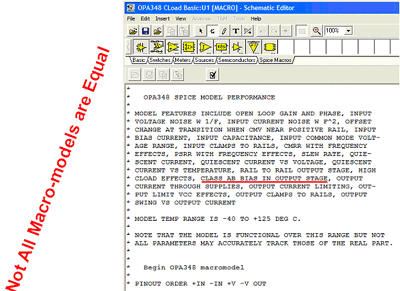
Figure 7.6: Not all SPICE amplifier models are equal !
Since we could not find a bipolar emitter follower amplifier macro model with accurate class AB biasing and real transistor outputs to perform accurate performance analysis in real environments , we built our own evaluation model. Here we can see an ideal front end implemented by a voltage-controlled voltage source with an open-loop gain of 160dB (x100E6). The output transistors QP and QM are in a simplified class AB bias circuit. We set the maximum output current of the amplifier to 27mA . Therefore, to find the R O parameter R X , we will test with a load current of +27mA . By using the "input resistor" RL and the "feedback" inductor LF , a simple Z O test circuit can be easily built in Tina SPICE . It is shown in Figure 7.7 . We can treat the inductor as a short circuit in the DC environment, and the voltage VDC is applied to RL , resulting in a DC load current as shown below . With an ideal 1T-Henry (1E12 Henry) inductor, we can achieve a DC closed loop path to allow SPICE to find the operating point , but it is an open circuit for any target AC frequency. Now, if we excite the circuit with an AC current source Itest of 1A , then the dB math conversion gives V OUT as Z O . Note that in this heavy load case, I OUT = +27mA , i.e. QM (actually in the "off" state) and QP (in the "on" state) determine the output impedance. Figure 7.7: Z O , Heavy Load I OUT = +27mA
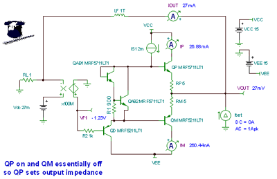
Figure 7.7 shows the measured results of Z O for a bipolar emitter follower output amplifier when I OUT = +27mA . The initial results from SPICE will be plotted in the "linear in dB " region. If we take the "logarithm" of the y -axis, this will directly produce the ohmic value of Z O. The logarithmic scale on the y -axis is helpful when we look at other Z O plots where the frequency bandwidth is not constant (such as CMOS RRO ) . 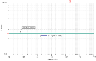
Figure 7.8: Z O AC plot, heavy load I OUT = +27mA
Figure 7.9 shows the large equivalent load Z O model at I OUT = +27mA . The measured value of R X is 6.39Ω . We assume that the QP and QM output transistors used are of similar performance and therefore assign the same R X value to both output transistors. If necessary, we can re-run the analysis and measure the R X value at I OUT = -27mA . The results will be so close that the difference can be ignored. Based on this model, we can assume that RMim is a high impedance and will not interfere with the measurement of R O. In addition, we assume that RPip is much smaller than R X.
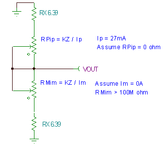
Figure 7.9: Heavy load Z O model Figure 7.10 details the no output load environment of the class AB biased emitter follower. We set the class AB bias current I AB to 1.08 mA . For the no output load condition, both output transistors QP and QM are on and have the same effect on Z O.
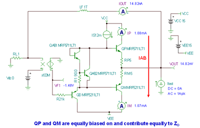
Figure 7.10: Z O , no-load I OUT = 0mA As shown in Figure 7.11 , the measured value of no-load Z O is 14.8 Ω . With this information and the heavily loaded value of Z O (inferred from R X ), we can complete the modeling of the small-signal Z O by calculating the constant K Z.
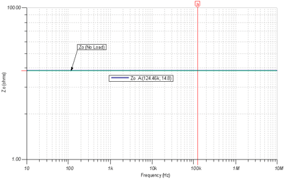
Figure 7.11: Z O AC diagram, no-load I OUT = 0mA In Figure 7.12 , we used the emitter follower Z O model under no-load conditions. We used the results obtained under heavy load conditions and filled in the corresponding value for R X. Now, we need to find the value of K Z for no-load conditions Z O , assuming that the parameters of the two output transistors QP and QM are similar. The detailed derivation process is shown in the figure above, and we find that the value of K Z is 0.0250668 .
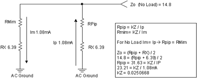
Figure 7.12: No-load Z O model Now, let's test the emitter follower Z O model. We will use a DC current from QP of about 2 times I AB , or twice the class AB bias current. This will turn off QM and force QP 's R O to dominate Z O. This is basically correct, as can be seen in Figure 7.13 . This also properly explains how the class AB bias scheme works in the real world. We learned that when the load current becomes positive, all the class AB bias current begins to shift toward the positive output transistor QP . When the load current becomes negative, all the class AB bias current begins to shift toward QM until QP is completely turned off by the negative heavy load current. 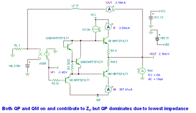
Figure 7.13: Z O , light load I OUT = +2xI AB (2.16mA) Figure 7.14 shows the emitter follower light load Z O model. Using the known R X and K Z values, we can calculate the equivalent Z O value required and then run a Tina SPICE simulation using the results in the figure below . We calculated that the Z O value under light load is 13.2326Ω , while the SPICE measurement result is 12.85Ω . The two results are very close and suitable for various related analysis. If we invest time to study, we will find that the parameters of QP and QM are not exactly the same. 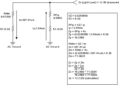
Figure 7.14: Light load Z O model Figure 7.15 shows the Tina SPICE simulation results of Z O at light load
Figure 7.15 : Z O AC diagram, light load I OUT = +2.16mA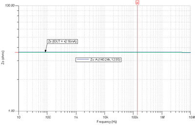
We can now build a complete set of emitter follower Z O curves as shown in Figure 7.16 . From Figure 7.16 we can see that Z O is determined by R O , which is constant for the unity gain bandwidth of the amplifier and decreases with increasing load current. Note that Z O is based on the light load condition of the source and drain current and that there is no significant difference in the source or drain Z O under heavy load conditions. These important Z O curves should be included in the bipolar emitter follower amplifier data sheet . 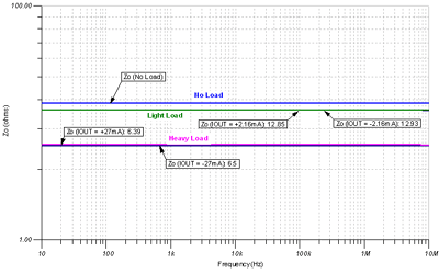
Figure 7.16: Complete Z O curve : bipolar emitter follower
Bipolar Emitter Follower Output Amplifier Z O and Capacitive Load
For the capacitive load of the emitter follower output stage , we will use the model in Figure 7.17 . We can look up the parameters from the product data sheet or obtain them by measuring the Aol curve of the amplifier without capacitive load. On the unloaded Aol curve of the amplifier , R O interacts with CL to form a second pole fp2 . 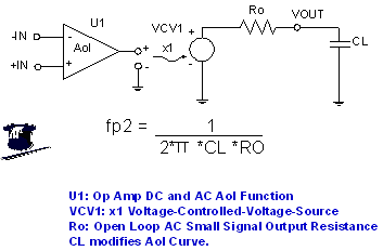
Figure 7.17: Bipolar emitter follower Z O and capacitive load We will apply many different capacitive loads to the emitter follower bipolar amplifier and measure the pole fp2 formed by the interaction of R O and CL . The circuit in Figure 7.18 uses LT as a DC short to establish the DC operating point. LT is open circuit for any selected AC frequency so that we can observe the modified Aol curve. CT is open circuit to DC but short circuit to target AC at any frequency , and CT also serves to connect the AC test source VG1 to the circuit. By inspection we find that Aol = VOA / VM .
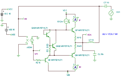
Figure 7.18: Tina SPICE circuit used to measure the modified Aol curve
Figure 7.19 shows the final modified Aol curve for various capacitive load conditions.
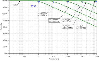
Figure 7.19: Modified Aol curves for different CL values
Figure 7.20 details the predicted positions of the fp2 poles caused by R O and CL in the modified Aol curve. The figure also shows the actual Tina SPICE measured positions corresponding to each fp2 . Due to the use of stable synthesis technology, the actual values of fp2 measured by Tina SPICE are not significantly different from our predicted values.
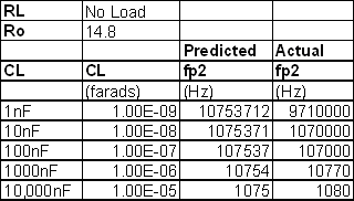
Figure 7.20: fp2 position for different CLs : predicted and actual values
Summary of Bipolar Emitter Follower Output Amplifier Z O
Figure 7.21 summarizes the bipolar emitter follower amplifier Z The key parameter of IOUT is the Z O. Within the unity-gain bandwidth of the amplifier, Z O is determined by R O and is constant with respect to frequency. As the DC output load current increases, R O decreases and becomes inversely proportional to I OUT . Capacitive load, CL , and R O interact to form a second pole, fp2 , on the original amplifier Aol curve . We can use the modified Aol curve to consider the appropriate closed-loop compensation value for better stability. R O will change with process and temperature variations. The rule of thumb for process and temperature variations is 0.65* R O typ (-55C) to 1.5* R O typ (125C) , where R O typ is the typical value of R O at 25C . The rule of thumb we have developed does not always apply to the open-loop output impedance of bipolar emitter follower amplifiers. The most complete and accurate Z O data can be obtained from the amplifier manufacturer or measured.
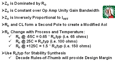
Figure 7.21: Summary of bipolar emitter follower Z O CMOS RRO ( Rail-to-Rail Output ) Amplifier Z O
Figure 7.22 shows a typical CMOS RRO amplifier topology. In this type of output stage , R O ( small signal, open loop output resistance ) is usually the main component of Z O ( small signal, open loop output impedance ) . R O is inversely proportional to most DC load currents. However, at light load currents, R O is directly proportional to the DC load current. In the low and medium frequency regions, Z O usually appears capacitive. Because RL (resistive load at the output) interacts with the capacitive part of Z O , the amplifier Aol curve will be affected in the low frequency region.
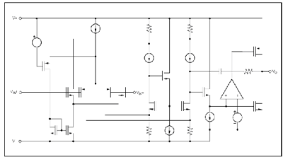
Figure 7.22: Typical CMOS RRO amplifier Figure 7.23 lists the relevant parameters using a CMOS RRO amplifier as an example. The OPA348 is also an RRI ( rail-to-rail input ) amplifier. The CMOS RRIO (rail-to-rail input / output) topology is ideal for single-supply applications with the following characteristics: small swings on the input and output rails, very low quiescent current, and very low input bias current. Its noise is usually much higher than that of a bipolar emitter follower amplifier.
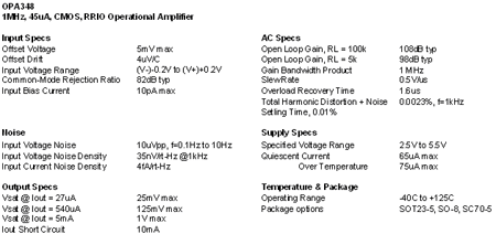
Figure 7.23: Example parameters : CMOS RRIO amplifier
Figure 7.24 is a simplified model we have drawn for a typical CMOS RRO amplifier that uses a voltage output differential front end with a controllable current source GM2. GM2 drives RO , which generates a voltage that controls the output current source GMO . Capacitor CO is fed back to the RO , GM2 junction. From this simplified model, we can see that at high frequencies , Z O = RO . As the frequency changes from high to mid and low frequencies, we will see the effect of CO , and Z O will also become capacitive. 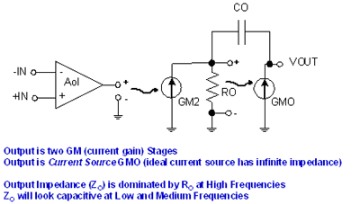
Figure 7.24: Simplified model : CMOS RRO amplifier As shown in Figure 7.25 , for most CMOS RRO amplifiers , when the amplifier output is unloaded , the class AB bias current of the output stage is approximately ? of the total amplifier quiescent current . At high frequencies , Z O = R O . R O is proportional to gm ( the current conversion rate of the MOSFET ). However, the gm of the MOSFET is inversely proportional to the square root of ID ( drain current).
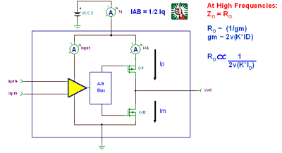
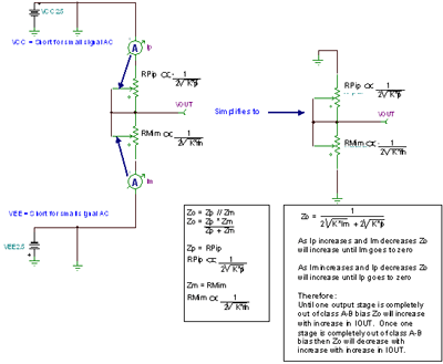
Figure 7.25: Z O Definition : CMOS RRO Amplifier Figure 7.26 details the CMOS RRO R O model , which consists of current control resistors for half-push (QP) and pull (QM) output MOSFETs . Each current control resistor, RPip and RMim, is proportional to the square root of the drain current on the corresponding MOSFET . When fed back to the output of the amplifier, the two current control resistors are in parallel, with a corresponding value of R O . The parallel equation of these resistors allows a mathematical equation to be established, which unexpectedly leads to a transfer function. When I OUT increases by a small amount, R O will continue to increase until one of the output MOSFETs is completely turned off and exits Class AB mode. Figure 7.26: R O Model: CMOS RRO Amplifier
The calculation example in Figure 7.27 shows the unique relationship between R O and small changes in I OUT . In class AB bias mode, when the current flowing through both devices, QP and QM, is 22uA , R O is equal to 200Ω . The increase in Im means that the current flowing into the amplifier output of I OUT is also increasing, and the current received by QP gradually decreases until it is completely turned off when Im = 44μA . At this time, R O is the maximum value (R O Max = 282.25Ω) . As the I OUT current increases, R O will decrease. 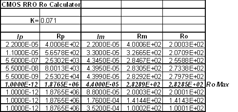
Figure 7.27: Example of R O increase / decrease parameter We have chosen the OPA348 , a CMOS RRIO amplifier, to investigate the CMOS RRO Z O . This device has a very accurate SPICE macro model and its Z O parameters have been evaluated in the lab. Tina SPICE makes it easy to view Z O parameters. For the first Z O measurement we will use a maximum load current of 10 mA . Note that the purpose of the current meter I OUT in the test circuit shown in Figure 7.28 is to ensure that the DC value of I OUT is accurately controlled to 10 mA . Simply dividing V1 by RL does not fully resolve the parameter problem of the amplifier input offset voltage and may cause unexpected errors.
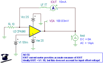
Figure 7.28: Z O , heavy load, I OUT = +10 mA
The AC diagram of Z O with I OUT equal to 10 mA includes a high frequency RO component of 34.79 Ω . Z O is clearly capacitive in the frequency band below 10 kHz . We speculate that the output current of RO is the lowest because QM is completely off and all the output stage current flows through QP .
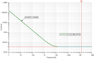
Fig. 7.29: Z O AC diagram, heavy load I OUT = +10mA
The heavy load R O model in Figure 7.30 illustrates that : R O 's output current is the lowest because QM is completely turned off and all the output stage current flows through QP .
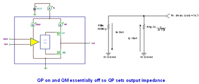
Figure 7.30: Heavy load R O model
We will use the circuit in Figure 7.31 to calculate the no-load Z O curve. According to the rule of thumb for the relationship between I Q and I AB , I Q = 45 μA in the OPA348 , so I AB = 22.5 μA . The error current of 483.65 fA will not have a significant effect on the no-load Z O curve.
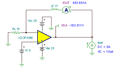
Figure 7.31: Z O , no load I OUT = 0mA
As shown in Figure 7.32 , Z O contains a high-frequency R O component of 196.75 Ω when I OUT equals 0 mA . Z O is obviously capacitive in the frequency band below 3kHz . 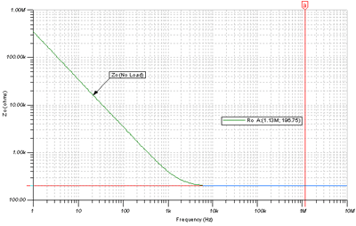
Fig. 7.32: Z O AC diagram, no load I OUT = 0mA
The no-load R O model in Figure 7.33 shows that the output QP and QM in the OPA348 have the same effect on R O. The figure also assumes that the class AB bias current is 22.5μA .
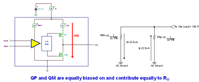
Figure 7.33: No-load R O model
We now know what Z O means for heavy load and no load. Another key curve we are interested in is the light load where R O becomes maximum. We don't know exactly where this operating point is because we can't see into the OPA348 class AB bias stage, but we need to know where it is before we can calculate the AC transfer curve. Using the technique and circuit in Figure 7.34 will quickly accomplish this. If we continue to run the AC Analysis / Calculate AC Node Voltage Analysis as shown , we can change the value of V1 and quickly update VOA . VOA is read as an RMS value . We set IG1 to 1A , AC generator, f = 1MHz (which is well within the frequency range where R O dominates Z O ) . Once we find the value of V1 that produces the maximum VOA , we can use it to calculate the AC transfer curve. Note: VOA is read as an RMS value , which includes all DC components of VOA . Also note: With respect to current levels, the DC value will drop in the 7.35μVrms region , which is not significantly different from VOA in the 254.56Vrms region. The AC amplitude value of R O at light load is 254.56Vrms/.707Arms = 360Ω ( AC sine wave Arms = 0.707Ap ).
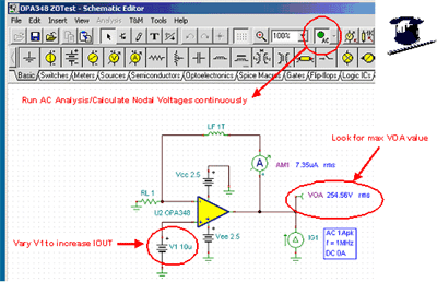
Figure 7.34: Seeking maximum R O with light load Figure 7.35 shows the Z O light load test circuit.
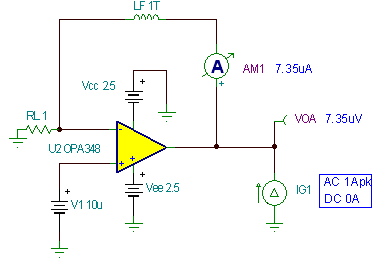
Fig. 7.35: Z O , light lLoad, I OUT = +7.35uA
Figure 7.36 shows the results of a light-load AC transfer function analysis of Z O. It shows our predicted 360Ω R O , with Z O becoming capacitive below about 3kHz . 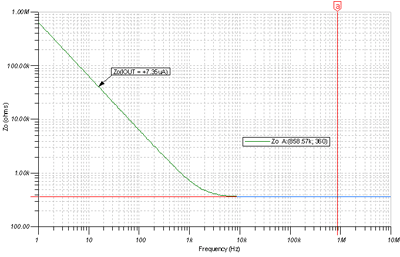
Figure 7.36: Z O AC diagram, light load I OUT = +7.35mA The light load model ( shown in Figure 7.37 ) has QP turned on and QM turned off . QP, because of its lowest impedance, will determine the value of R O. The initial assumption of a class AB bias current of 22.5 μA may not be correct, because only 7.35 μA of load current is required to turn QM off. IAB may not be much greater than 7.35 μA . 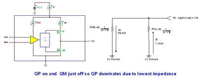
Figure 7.37: Light load Z O model
Figure 7.38 shows the complete set of Z O curves for the OPA348 . The key curves we are concerned about include: I OUT = +7.35uA (R O = 360 Ω à R O max ) I OUT = +7.35uA (R O = 196.75 Ω à R O no load ) I OUT = +87.4uA (R O = 198.85 Ω ) , at this I OUT value, R O is approximately equal to R O no-load. ? I OUT > 87.4μA results in R O < R O no load I OUT = +10mA (RO = 34.79 Ω )
The other curves shown are only for verifying operation between the critical curves. In addition, the Z O curve can be used to determine I OUT for negative current values . However, in the positive region of the current curve, these curves are too closely spaced to be placed on top of I OUT , so they are omitted to ensure clarity of the chart. All CMOS RRO amplifier data sheets should include these critical Z O curves.
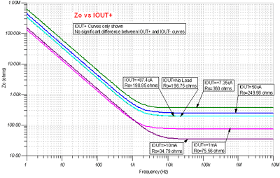
Figure 7.38: Complete Z O curve : CMOS RRO
To build an equivalent Z O model for an RRO CMOS amplifier , we need to analyze the breakpoints fz on the Z O curve . Figure 7.39 shows the measured values of these breakpoints under heavy load and no load. The CO value can be determined based on the frequency and R O value .
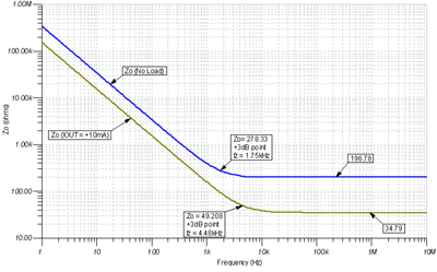
Figure 7.39: Breakpoint fz on the Z O curve
Using the Z O plot, the Z O model for a given I OUT load at no load and heavy load (10 mA) can be completed as shown in Figure 7.40 .
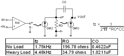
Figure 7.40: Z O full model calculation
Z O and Capacitive Loading of CMOS RRO Amplifiers
If the modified Aol curve is established from the initial amplifier Aol , the load capacitor CL will be in series with the Z O model capacitor CO when driving a capacitive load . Note that the calculation of the series capacitance value is similar to the calculation of the parallel resistance value. Therefore, if CL < CO , then CL is dominant; if CL > CO, then CO is dominant. The second pole of the modified Aol curve , fp2, is directly related to R O and Ceq ( the equivalent capacitance of CO and CL ) . Figure 7.41 shows these key points. 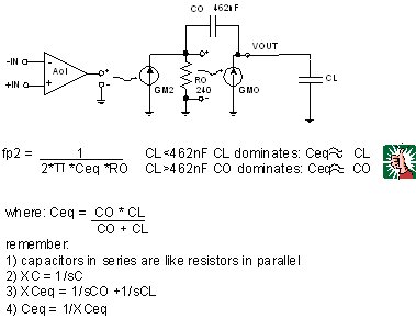
Figure 7.41: Corrected calculation of Aol fp2
Figure 7.42 is a test circuit used to correct the Aol curve for capacitive loads in a CMOS RRO amplifier . LT opens the AC loop, but LT provides a short circuit in the DC operating point calculation. CT is an open circuit to DC and a short circuit to AC at any set frequency . The corrected Aol curve is VOA / VM .
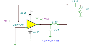
Figure 7.42: Modified Aol test circuit Figure 7.43 shows the true corrected Aol curve for CL from no load to 10,000nF . The measured values at the corresponding positions of fp2 are marked in the figure.
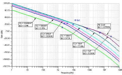
Figure 7.43: CL Corrected Aol Curve
Figure 7.44 compares the measured fp2 values to the Z O model predictions. The results show that we can confidently use the Z O model to predict the true modified Aol plot. Note that the 1nF load prediction error is large because we do not consider the effect of the second high frequency pole (2.87MHz) of the OPA348 Aol . Because CL is too far from 2.87MHz, another fp2 location can be determined , so the second pole of the OPA348 Aol has no effect on the prediction.
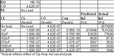
Figure 7.44: Comparison of the predicted and true values of the modified Aol fp2
Low-frequency Effect of RL on CMOS RRO Amplifier Aol
Just when we thought we were done with CMOS RRO amplifiers … Another low-frequency Aol phenomenon also occurs with CMOS RRO amplifiers . The interaction of CO and RL produces a high-pass filtering effect that flattens the low-frequency portion of the Aol curve (see Figure 7.45 ).
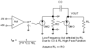
Figure 7.45: Aol low frequency effect of RL
Figure 7.46 is a test circuit for analyzing the effect of RL on the CMOS RRO Aol curve. It is easy to observe the effect on Aol by adjusting the RL size .
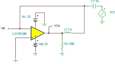
Figure 7.46: Aol low frequency effect of RL test circuit
Figure 7.47 clearly shows the low-frequency Aol effect for no-load, 100kΩ , and 5kΩ resistive loads .
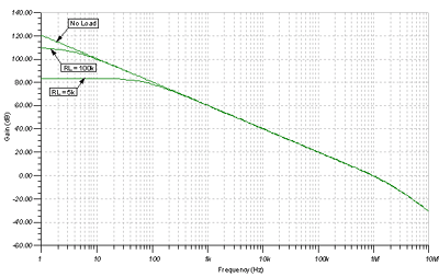
Figure 7.47: AC diagram of RL effect in the low frequency part of Aol
The test circuit in Figure 7.48 allows us to see the effect of CO and RL on the low frequency region of the CMOS RRO Aol curve. Vaol represents the unloaded, uncorrected Aol curve. VHP is the high pass filtering effect produced by CO and RL . VOA is the corrected Aol curve produced when the uncorrected Aol curve passes through the high pass filter formed by CO and RL . 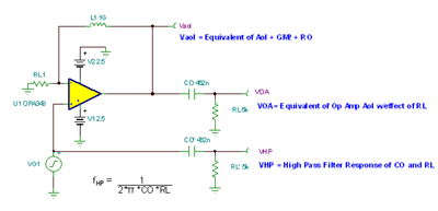
Figure 7.48: Equivalent circuit for evaluating the RL effect on Aol
Figure 7.49 is the comprehensive AC curve when RL = 5k Ω , showing the uncorrected Aol curve Vaol , the high-pass filter effect and network transfer function of CO and RL , and the corrected Aol curve VOA generated by Vaol through VHP . Since addition on the Bode diagram is equivalent to linear multiplication, we only need to add Vaol and VHP to get the VOA curve.
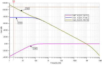
Figure 7.49: Equivalent circuit diagram for evaluating the RL effect on Aol
Summary of Z O of CMOS RRO Amplifiers
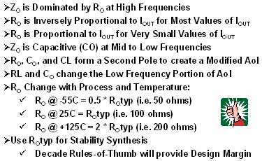
Figure 7.50 summarizes the key parameters of the CMOS RRO amplifier , Z O. At high frequencies, Z O is determined by R O. For most loads, as the DC output load current increases, R O decreases and becomes inversely proportional to I OUT . However , at low I OUT , R O is proportional to I OUT . In the low- to mid-frequency region, Z O is the capacitive CO . If a capacitive load CL is connected to the CMOS RRO output, R O and CO will interact with CL and produce a modified Aol curve with an additional pole, fp2 , compared to the original Aol curve . The low-frequency portion of the Aol curve is affected by the resistive load RL , which interacts with CO to form a high-pass filter effect, making the Aol curve flat in the low- to mid-frequency region . R O varies with process and temperature. The rule of thumb for process and temperature variations is 0.5 × R O typ (-55C) to 2 × R O typ (125C) , where R O typ is the typical value of R O at 25C . The rules of thumb we have developed do not always apply to the open-loop output impedance of CMOS RRO amplifiers. The most complete and accurate Z O data should be obtained from the amplifier manufacturer or through measurement.
| 


 Room 1530, Zhongguancun MOOC Times Building,
Block B, 18 Zhongguancun Street, Haidian District,
Beijing 100190, China
Tel:(010)82350740
Postcode:100190
 京公网安备 11010802033920号


 提升卡
提升卡 变色卡
变色卡 千斤顶
千斤顶