|
The OP
Published on 2019-7-25 20:44
Only look at the author
This post is from Microcontroller MCU
| ||
|
|
||
- 【Posts】Get accurate, fast and stable analog voltage from digital PWM signal
- 【Posts】Is there any chip that can convert analog signal (potentiometer and DC voltage) into PWM dimming signal?
- 【Posts】IO simulates PWM, 4.2V power-on duty cycle 100%, but the load voltage is only 3.55V
- 【Posts】PMOS is used as PWM switch power supply. The output PWM voltage signal has negative voltage overshoot voltage for too long. Please solve it.
- 【Posts】The microcontroller outputs PWM wave to control the load supply voltage 0-12V adjustable
- 【Posts】There are several problems when ADC samples two sets of DAC output voltages, as shown in the figure. In addition, if the signal is about 1uA, does it need 20 bits?
- 【Posts】The DC power supply output voltage is unstable. How to calibrate and test it?
- 【Posts】How to process the weak AC signal collected by the voltage transformer and the amplified signal after being amplified and biased by the operational amplifier?
- 【Download】MSP430 MCU drives 1602 LCD, generates PWM output, realizes RS232 communication, digital voltmeter, signal generator
- 【Download】How to quickly and accurately locate anomalies in analog signals during performance verification
- 【Download】Stable Control Strategy for DC Link Voltage of Dual PWM Controlled AC Excitation Power Supply
- 【Download】Using a broadband automatic gain control circuit, the OPA660 can change the signal amplitude and keep the output signal stable within the input voltage range.
- 【Design】FAN65008B-GEVB: High Performance 65V, 10A Voltage Mode Synchronous PWM Buck Regulator Evaluation Board
- 【Design】FAN65005A-GEVB: High Performance 65V, 8A Voltage Mode Synchronous PWM Buck Regulator Evaluation Board
- 【Design】FAN65004B-GEVB: High Performance 65V, 6A Voltage Mode Synchronous PWM Buck Regulator Evaluation Board
- 【Design】[Analog circuit] 431 reference voltage source
- 【Design】8-Channel Isolated High-Voltage Analog Input Module Reference Design Using ISOW7841
- 【Design】CARMEL (MAXREFDES18#): High-precision analog current/voltage output
- 【Circuits】Analog voltmeter circuit with digital input
- 【Circuits】Use three voltage regulator star connections to obtain 0-433V voltage circuit diagram
- 【Circuits】Obtaining two voltages from one rectifier circuit
- 【Circuits】3.5V power supply, stable low voltage, low power consumption reference voltage generation circuit
- 【Circuits】Circuit diagram of stable and adjustable negative output voltage composed of NE555
- 【Circuits】Converter circuit diagram using magnetic amplifier to stabilize voltage
- 【Articles】Method for obtaining analog voltage reference value using mixed signal device
- 【Articles】A method for quickly generating analog voltage based on PWM
- 【Articles】Analog/digital converter using low voltage differential signaling data bus
- 【Articles】PWM reference voltage generation circuit with accurate step voltage
- 【Articles】Stable, fast and accurate, simple DC electronic load for measuring large current and voltage
- 【Articles】51 MCU uses timer interrupt to simulate PWM control port voltage
-
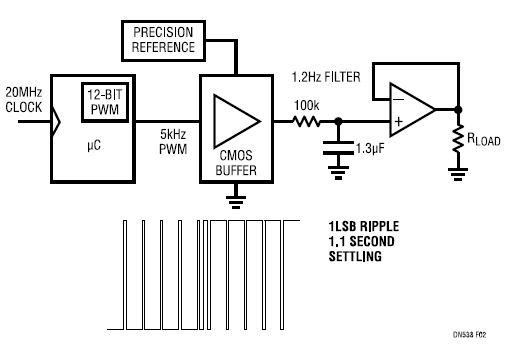
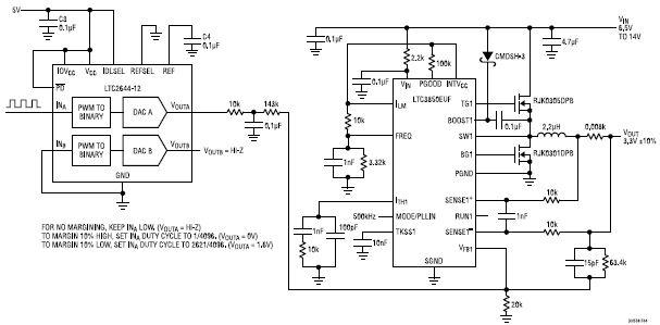
Get accurate, fast and stable analog voltage from digital PWM signal
PulseWidthModulation(PWM)isacommonmethodtogenerateanalogvoltagesfromdigitaldevicessuchasmicrocontrollersorFPGAsIftheperformancerequirementsoftheanalogsignalarenottoostringent,thisisasimpleandpracticalmethodbecauseitonlyrequiresoneoutputpina ...
-
Is there any chip that can convert analog signal (potentiometer and DC voltage) into PWM dimming signal?
[align=left]Isthereanychipthatcanconvertanalogsignals(potentiometerandDCvoltage)intoPWMdimmingsignalsalign]
-
It's really fast. It's already snowing today~~~
Nothingmuch,IjustwisheveryoneahappyXiaoxue~~~
- What are the advantages of fiber optic through-beam sensors and what are their working principles and applications?
- Global and China Ferrophosphate Rotary Kiln Roasting Furnace Market Share and Ranking Analysis Report
- Moto Bluetooth Headset HS810 Disassembly [Multiple Photos]
- 【NXP Rapid IoT Review】+⑦NXP Rapid IoT Review Summary
- Microchip Elite Technology Annual Conference (2009--2017)
- Fluke and universities jointly build laboratories
- TI's C6000 series DSP, implementation of flashboot
EEWorld Datasheet Technical Support
-
Europe's three largest chip giants re-examine their supply chains
At the Electronica 2024 CEO Roundtable held just last week, the CEOs of three chip giants, Infine
-
It is reported that Kioxia will be approved for listing as early as tomorrow, and its market value is expected to reach 750 billion yen
On November 21, Reuters reported that with the support of Bain Capital, Kioxia will obtain approv
-
The US government finalizes a $1.5 billion CHIPS Act subsidy to GlobalFoundries to support the latter's expansion of production capacity in the US
On November 21, the U.S. Department of Commerce officially announced yesterday that it will provi
- SK Hynix announces mass production of the world's highest 321-layer 1Tb TLC 4D NAND flash memory, plans to ship it in the first half of 2025
- UWB is a new way to use it in cars. Can wireless BMS also use it?
- Filling the domestic gap! China Mobile, Huawei and others jointly released the first GSE DPU chip
- Samsung Electronics NRD-K Semiconductor R&D Complex to import ASML High NA EUV lithography equipment
- Apple reveals the secret of its own chip success: competitors can't use the latest cutting-edge technology
- A big chip war is about to start: Qualcomm and MediaTek are involved in notebooks, and AMD is reported to enter the mobile phone market
- Exynos 2600 chip is the key, Samsung is reportedly going to launch a 2nm chip counterattack
- Problems with STM32 and passive buzzer playing sound
- Embedded Tutorial_DSP Technology_DSP Experiment Box Operation Tutorial: 2-28 Building a Lightweight WEB Server Experiment
- OPA847IDBVR op amp domestic replacement
- AG32VF407 Test UART
- [Digi-Key Follow Me Issue 2] Chapter 1: Sharing on receiving the goods
- What model is this infrared receiver? Which model can be used instead? Thank you
- Selling brand new unopened ZYNQ 7Z020 FPGA core board
- The LORA module used in the lithium battery-powered water meter setting can save energy when 100 water meters are installed in one corridor.
- I would like to ask, when a port is set to RX0, is it necessary to set the input and output direction of this port?
- Why is this year so difficult? It’s even more difficult than during the pandemic. I’m 30 and facing unemployment. I’m so confused.
- Ask about the voltage regulator test question
- [Xiaohua HC32F448 Review] About Xiaohua Semiconductor's UART interrupt sending and PRINTF construction and redirection
- 【BIGTREETECH PI development board】 HDMI output test
- 【BIGTREETECH PI development board】+08. Audio test (zmj)
- [Xiaohua HC32F448 Review] +RTC electronic clock
- 有奖直播报名| 高可靠性IGBT新选择 —— 安世半导体650V IGBT
- 【直播时间】12月19日(周四)下午15:00-16:30
【直播好礼】定制双肩商务包、30元京东卡、吸管玻璃杯
- 安世半导体直播报名中
- 直播主题:安世半导体理想二极管与负载开关,保障物联网应用的稳健高效运行
直播时间:12月17日(周二)下午14:00
报名就有机会获得:定制双肩商务包、30元京东卡、吸管玻璃杯
- PI 电源小课堂 | 无 DC-DC 变换实现多路高精度输出反激电源
- 时间:即日起-12月15日
看视频学习电源干货,答题赢取京东卡!
- 参会有好礼 | 2024 瑞萨电子MCU/MPU工业技术研讨会
- 深圳站:11月30日(周六)深圳湾万怡酒店
上海站:12月06日(周五)上海喜玛拉雅酒店
奖励设置:现金红包、螺丝刀套装或30元京东卡
- Littelfuse 新品赋能电子产品安全可靠并高效, 10+挑战等你探索!
- Littelfuse 应用赋能星球,覆盖了诸多应用痛点及解决办法,邀请工程师一起探索,解锁更多设计力!
- 下载资料赢好礼!看Vicor模块化电源解决方案如何推动创新
- 活动时间:即日起-2024年12月31日
如何参与:点击活动页内您想了解的模块,找到资料下载即可参与抽奖,活动结束后统一发奖!
- 有奖活动|英飞凌高密度双相电源模块为高性能运算平台而生
- 活动时间:即日起-12月15日
活动奖励:蓝牙音箱、氮化镓充电器套装、黑色小背包
- 本周精选下载推荐:电源管理基础Dummies
- 本周小编给大家带来一本超简单、超干货的电子书——《电源管理基础Dummies》!内容深入浅出,排版舒服简洁,分分钟能get到电源管理最核心的知识内容。
EEWorld
subscription
account

EEWorld
service
account

Automotive
development
circle

About Us Customer Service Contact Information Datasheet Sitemap LatestNews
- I want to get started with PIC microcontrollers, what should I do?
- I want to get started with Xilinx deep learning, what should I do?
- Please recommend some good neural network introduction
- For beginners of machine learning keras, please give a learning outline
- For a classic introduction to machine learning, please give a study outline
- Please give a learning outline for getting started with the deep learning tool tensorflow
- What textbooks should machine learning beginners use?
- What microcontrollers should I learn for beginners?
- Which country is the RISC-V architecture from?
- Is AI computing power GPU or CPU?


 Room 1530, Zhongguancun MOOC Times Building,
Block B, 18 Zhongguancun Street, Haidian District,
Beijing 100190, China
Tel:(010)82350740
Postcode:100190
 京公网安备 11010802033920号


 提升卡
提升卡 变色卡
变色卡 千斤顶
千斤顶