How to Make a PIC Programmer
Source: InternetPublisher:笑流年 Keywords: PIC Programmer Updated: 2024/11/15
1. Circuit principle of PlC programmer
Since the PIC microcontroller has multiplexing functions for its I/O (input, output) port, a function called "in-circuit serial programming (ICSP)" is provided on the I port. Even after the chip is soldered to the circuit board, it can realize the programming (burning) function of the PIC microcontroller through simple connections. This programming interface only uses 5 wires of the chip pins: +5V power supply - connected to the chip VDD pin, reference ground - connected to the chip Vss (GND), programming voltage - connected to the chip MCLR/VPP pin, serial programming data PGD - connected to the chip RB7 and serial programming clock PGC - connected to the chip RB6 pin. Note: For the configuration of the serial programming data and clock pins of the 8- and 14-pin packaged chips of the PIC chip, please refer to the markings on the PIC microcontroller data sheet. All PIC microcontroller basic and intermediate products (including one-time programmable OTP chips) have the function of in-circuit serial programming. In fact, the commonly used programmers also use this ICSP-in-circuit serial programming function when burning and programming chips. According to the above, when programming on many PIC chip pins, only the above five pins will be used, as shown in Figure 2. As can be seen from Figure 2, the ICSP (In-Circuit Serial Programming) programming interface is so simple that readers can make their own programmers and program their own designed products.

2. PIC-18 pin dual in-line microcontroller programmer circuit diagram
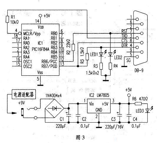
The programmer (burner) circuit made according to the ICSP function of the PIC chip in Figure 2 is shown in Figure 3. For the sake of convenience, only PIC-18 pin chips, such as PIC16F84A/16F627 microcontrollers, are used here to explain, and then extended to PIC multi-pin programmer circuits.
The PIC microcontroller chip programmer circuit in FIG3 connects the PIC chip in-circuit serial programming (ISCP) interface of FIG2 to a PC via a DB-9 socket of an RS-232 cable, and then configures a set of software platforms (described below) to form a self-contained system. At this time, only the specified operations on the PC are required to complete the programming (burning function) of the chip.
Figure 3 is the actual hardware circuit of the 18-pin programmer. The 5 pins of the chip used for the ICSP function of the PIC chip described in Figure 2 are connected to the RS-232 cable DB-9 socket as follows: RB7/PCD is connected to the ⑧ pin of the DB-9 socket and the ④ pin through R5; RB6/PGC is connected to the ⑦ pin of DB-9 through resistor R2; MCLR/VPP (programming voltage) is connected to the ③ pin of DB-9 through resistor R1 and VSS (signal ground) is connected to the ⑤ pin of DB-9 (signal ground). When programming (burning), the power supply VDD of the PIC microcontroller is powered by the +5v power supply in Figure 3.

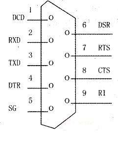
The +5V power supply in Figure 3 is a most common LM7805 voltage-stabilized power supply circuit. The input of this power supply is a +9V power adapter purchased from the electronics market (i.e. 220V input, +9V DC output), and a +5V voltage-stabilized output is obtained for the VDD of the PIC chip. When the +5V power supply is working normally, the indicator LED3 is always on. As for the pin functions of each pin of the PIC chip online programming (ICSP) connected to the DB-9 socket, they are shown in Figure 4.

DB-9 is a connector plug in the RS-232C serial communication standard, used for asynchronous communication with a PC. There are 9 signals on the DB-9 connector, and when the PIC chip is connected to the DB-9 connector during in-circuit serial programming (ICSP), only 5 pins of DB-9 are used, as shown in Figure 3 above, which are pins ⑧, ⑦, ③, ④, and ⑤ of DB-9. The functions of the five pins are described as follows: RTS7 represents request to send, that is, when the data terminal needs to send data, RTS is first valid (ON state); CTS8 represents clear to send, that is, the response signal of the data communication device to the request to send signal RTS. When CTS is valid (ON state), it indicates that the data communication device is ready to receive its data; TXD3 represents the data transmission line (Transmitted Data), that is, the data terminal sends the serial data (here is the programming voltage Vpp) through TXD; DTR4 represents data terminal ready (Data Terminal Ready), that is, the data terminal ready signal. When DTR is valid (ON state), it notifies the data communication device that its data terminal can be used; SG5 represents the signal ground.
Here, the remaining pins of the DB-9 connector, Rl (pin 9), DSR (pin 6), RXD (pin 2) and BCD (pin 1), are not used during the "online serial programming" of the microcontroller.
The light-emitting diodes LED1 and LED2 in the circuit of Figure 3 and their current-limiting resistors R3 and R4 form a flashing display when the programmer burns the target code (.hex), which can directly observe the normal working process of burning the chip. When the burning work is completed, LED1 and LED2 go out. If LED1 and LED2 do not flash during the process of burning the chip, it means that there is a fault in the burning circuit board or the burning operation is improper, so that the user can find the fault.
3. PlC single chip multi-pin programmer circuit diagram
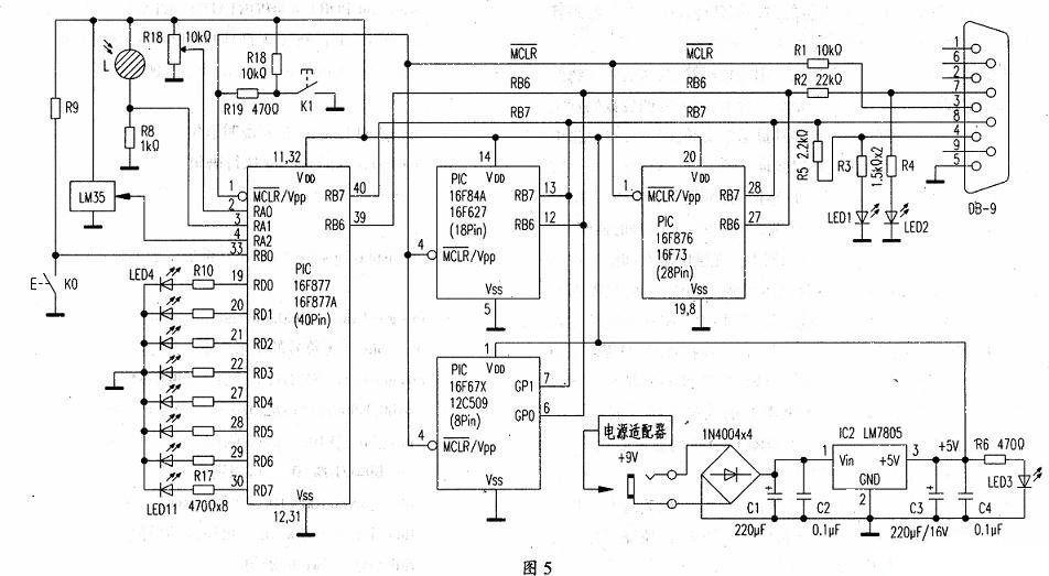
According to the circuit principle of the PIC programmer and the circuit diagram 3 of its 18-pin dual in-line microcontroller programmer, it is easy to draw the circuit diagram of the PIC microcontroller multi-pin programmer, as shown in Figure 5. The multi-pins here refer to the 8, 18, 28 and 40 pins of the PIC microcontroller dual in-line type.
The maker only needs to connect the programming voltage Vpp terminal, serial programming data PGD terminal, serial programming clock PGC terminal and signal ground line of PIC-40-pin microcontroller (such as PIC16F877), 28-pin microcontroller (such as PIC16F73), 18-pin microcontroller (such as PIC16F84A) and 8-pin microcontroller (such as PIC12F67X) in parallel (refer to MCLR/Vpp, RB7, RB6, GPO, GPl in Figure 5) to form the ICSP interface line of the PIC microcontroller in Figure 2. Then connect these interface lines to the corresponding pins of the RS-232 cable DB-9 socket in the manner of Figure 3, and then connect R4, LED1, R3, LED2 and +5V power supply, etc., to form the multi-pin programmer circuit diagram of the PIC microcontroller in Figure 5.
In Figure 5, the external components and LEDs such as RAO-RA2, RBO, RDO-RD7 in the PIC-40 pins serve as the A/D conversion experiment board circuit diagram for burning the PIC-40 pin chip.

- Interface circuit between intelligent temperature sensor TCN75 with two-wire serial interface and 89C51 single-chip microcomputer
- Interface circuit based on 8155 and single chip microcomputer
- How to make a BLE-enabled smart light bulb using STM32
- How to control fans using LM35 and ATTiny13
- How to use ESP32 to implement the design of air quality monitoring system
- How to use ADXL335 to realize the design of gesture control robot
- Use PC’s RS232 port to control LED lights
- SST89C58 electronic disk circuit and code
- 815 motherboard
- 815e motherboard


 京公网安备 11010802033920号