|
The OP
Published on 2019-8-9 21:54
Only look at the author
This post is from Microcontroller MCU
| ||||||||||||||||||||||||||||||||||||
|
|
||||||||||||||||||||||||||||||||||||
- 【Posts】Implementation Method of Software Serial Interface (SCI) Based on C2000
- 【Posts】C2000 Software Serial Interface (SCI) Implementation Method
- 【Posts】關於C2000 使用SCI在線升級做法求解
- 【Posts】C2000 MCU implements some strategies for motor control using the execution software stack
- 【Posts】MATLAB APP Designer serial port debugging tool writing
- 【Posts】AUTOSAR software development learning complete set of materials
- 【Posts】My own feelings about simulation software
- 【Posts】The serial port assistant can receive commands, but when connected to the light source, the light source does not respond. Why?
- 【Download】TMS320LF2407_SCI programming to achieve serial communication with PC
- 【Download】Questions and answers about 2407\'s SCI serial port expansion to achieve DSP serial communication and address
- 【Download】Design of serial device communication implementation method in configuration software
- 【Download】4-C2000 software programming method
- 【Download】Verilog^VHDL code conversion software XHDL-4.2.1, with cracking method and software
- 【Download】[C language interface and implementation: technology for creating reusable software]. (Hanson). Guo Xu. Scanned version
- 【Download】Ideas and methods of embedded software design
- 【Download】C8051F implements AD and serial port transmission and reception program at the same time.doc
- 【Design】A low-profile version of full-featured software radio based on Raspberry Pi Pico (fully open source + detailed explanation)
- 【Design】Infineon xc2000 MCU programming adapter board
- 【Design】Vienna rectifier-based three-phase power factor correction reference design using C2000 MCU
- 【Design】Two-phase interleaved LLC resonant converter reference design using C2000 MCU
- 【Design】EnDat 2.2 Absolute Encoder Master Interface Reference Design for C2000 MCUs
- 【Design】Vienna Rectifier-Based Three Phase Power Factor Correction Reference Design Using C2000 MCU
- 【Circuits】Serial debugger circuit implemented with several discrete components
- 【Circuits】USB-serial port conversion circuit made with CP2102 chip
- 【Circuits】RS232 transmission circuit between PC serial port and MC68HC70-5K1 microcontroller
- 【Circuits】Use PC serial port to read 16 digital input channel circuit diagram
- 【Circuits】51 microcontroller and PC serial port communication program and hardware circuit diagram
- 【Circuits】TOP6 Collection of Common Serial Port Interface Circuit Designs—Circuit Diagrams Read Every Day (118)
- 【Articles】Introduction to the method of realizing serial port simulation by microcontroller software
- 【Articles】Introduction to clever methods of 51 kernel software delay and serial port
- 【Articles】Freescale MC9S12XS128 SCI serial port related...
- 【Articles】Freescale 16-bit MCU (Part 7) - SCI serial port test
- 【Articles】[MCU Notes] Clever use of 51 kernel software delay and serial port
- 【Articles】Microcontroller study notes: 51 core software delay and serial port clever method
-
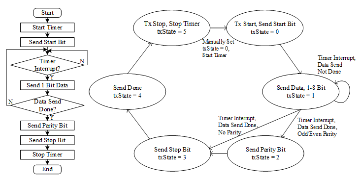
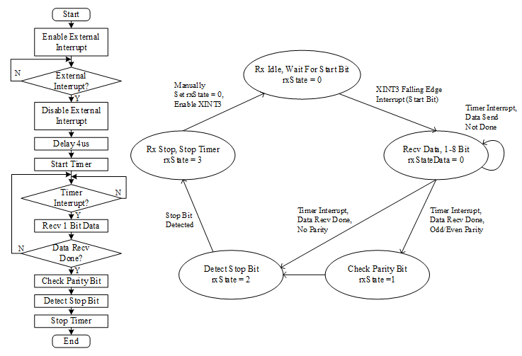
Implementation Method of Software Serial Interface (SCI) Based on C2000
introduction:TheC2000PiccoloseriesMCUchipsgenerallyintegrate1-2hardwareSCI(UART)Inthiscase,GPIOsoftwarecanbeusedtosimulatetheSCIinterface.ThisarticlegivesthemethodandroutinesofsimulatingGPIOintoSCIinterfacebyusingexternalinterruptandCPUtime ...
-
C2000 Software Serial Interface (SCI) Implementation Method
TheC2000PiccoloseriesMCUchipsgenerallyintegrate1-2hardwareSCI(UART)Inthiscase,GPIOsoftwarecanbeusedtosimulatetheSCIinterface.ThisarticlegivesthemethodandroutinesofsimulatingGPIOintoSCIinterfacebyusingexternalinterruptandCPUtimer.1.Testrelat ...
-
[V2S200D Voice Vibration Sensor Evaluation Kit Review] Review Summary
ThistimeIappliedtoparticipateintheevaluationof[V2S200DVoiceVibrationSensorEvaluationKit(KAS-33100-0007)]andwasfortunatelyselected:Evaluationshortlist:V2S200DVoiceVibrationSensorEvaluationKit(KAS-33100-0007).Afterreceivingtheevaluationkit,we ...
- [V2S200D Voice Vibration Sensor Evaluation Kit Review] Audacity Tool Test
- 【Follow me Season 2 Episode 4】IMU sensor six-axis data printing
- Tom filters sensitive Skype messages at the request of the Chinese government
- Energy saving: the driving force for continued growth in power management
- Libero IDE 7.2 increases flexibility for Actel FPGA-based designs
- Switching Power Supply Interest Group Task 03
- Introduction to Gizwits Mini Programs: WebSocket Web Page Control
EEWorld Datasheet Technical Support
-
"Cross-chip" quantum entanglement helps build more powerful quantum computing capabilities
IBM scientists have achieved "cross-chip" quantum entanglement - successfully entangled two "Eagl
-
Ultrasound patch can continuously and noninvasively monitor blood pressure
A research team at the University of California, San Diego, has developed an innovative wearable
-
Europe's three largest chip giants re-examine their supply chains
At the Electronica 2024 CEO Roundtable held just last week, the CEOs of three chip giants, Infine
- It is reported that Kioxia will be approved for listing as early as tomorrow, and its market value is expected to reach 750 billion yen
- The US government finalizes a $1.5 billion CHIPS Act subsidy to GlobalFoundries to support the latter's expansion of production capacity in the US
- SK Hynix announces mass production of the world's highest 321-layer 1Tb TLC 4D NAND flash memory, plans to ship it in the first half of 2025
- UWB is a new way to use it in cars. Can wireless BMS also use it?
- Filling the domestic gap! China Mobile, Huawei and others jointly released the first GSE DPU chip
- Samsung Electronics NRD-K Semiconductor R&D Complex to import ASML High NA EUV lithography equipment
- Apple reveals the secret of its own chip success: competitors can't use the latest cutting-edge technology
- Problems with STM32 and passive buzzer playing sound
- Embedded Tutorial_DSP Technology_DSP Experiment Box Operation Tutorial: 2-28 Building a Lightweight WEB Server Experiment
- OPA847IDBVR op amp domestic replacement
- AG32VF407 Test UART
- [Digi-Key Follow Me Issue 2] Chapter 1: Sharing on receiving the goods
- What model is this infrared receiver? Which model can be used instead? Thank you
- Selling brand new unopened ZYNQ 7Z020 FPGA core board
- The LORA module used in the lithium battery-powered water meter setting can save energy when 100 water meters are installed in one corridor.
- I would like to ask, when a port is set to RX0, is it necessary to set the input and output direction of this port?
- Why is this year so difficult? It’s even more difficult than during the pandemic. I’m 30 and facing unemployment. I’m so confused.
- Ask about the voltage regulator test question
- [Xiaohua HC32F448 Review] About Xiaohua Semiconductor's UART interrupt sending and PRINTF construction and redirection
- 【BIGTREETECH PI development board】 HDMI output test
- 【BIGTREETECH PI development board】+08. Audio test (zmj)
- [Xiaohua HC32F448 Review] +RTC electronic clock
- 有奖直播报名| 高可靠性IGBT新选择 —— 安世半导体650V IGBT
- 【直播时间】12月19日(周四)下午15:00-16:30
【直播好礼】定制双肩商务包、30元京东卡、吸管玻璃杯
- 安世半导体直播报名中
- 直播主题:安世半导体理想二极管与负载开关,保障物联网应用的稳健高效运行
直播时间:12月17日(周二)下午14:00
报名就有机会获得:定制双肩商务包、30元京东卡、吸管玻璃杯
- PI 电源小课堂 | 无 DC-DC 变换实现多路高精度输出反激电源
- 时间:即日起-12月15日
看视频学习电源干货,答题赢取京东卡!
- 参会有好礼 | 2024 瑞萨电子MCU/MPU工业技术研讨会
- 深圳站:11月30日(周六)深圳湾万怡酒店
上海站:12月06日(周五)上海喜玛拉雅酒店
奖励设置:现金红包、螺丝刀套装或30元京东卡
- Littelfuse 新品赋能电子产品安全可靠并高效, 10+挑战等你探索!
- Littelfuse 应用赋能星球,覆盖了诸多应用痛点及解决办法,邀请工程师一起探索,解锁更多设计力!
- 下载资料赢好礼!看Vicor模块化电源解决方案如何推动创新
- 活动时间:即日起-2024年12月31日
如何参与:点击活动页内您想了解的模块,找到资料下载即可参与抽奖,活动结束后统一发奖!
- 有奖活动|英飞凌高密度双相电源模块为高性能运算平台而生
- 活动时间:即日起-12月15日
活动奖励:蓝牙音箱、氮化镓充电器套装、黑色小背包
- 本周精选下载推荐:电源管理基础Dummies
- 本周小编给大家带来一本超简单、超干货的电子书——《电源管理基础Dummies》!内容深入浅出,排版舒服简洁,分分钟能get到电源管理最核心的知识内容。
EEWorld
subscription
account

EEWorld
service
account

Automotive
development
circle

About Us Customer Service Contact Information Datasheet Sitemap LatestNews
- I want to get started with Cadence PCB, what should I do?
- I want to get started with FPGA hardware design, what should I do?
- I want to get started with java neural network, what should I do?
- I want to get started with microcontroller systems, what should I do?
- For the introduction of tensor neural network, please give a learning outline
- For beginners, please give a learning outline
- For an introduction to neural network value functions, please give a learning outline
- How to get started with domestic single-chip microcomputers
- What software is generally used for fpga development
- The origin of the name Bluetooth


 Room 1530, Zhongguancun MOOC Times Building,
Block B, 18 Zhongguancun Street, Haidian District,
Beijing 100190, China
Tel:(010)82350740
Postcode:100190
 京公网安备 11010802033920号






 提升卡
提升卡 变色卡
变色卡 千斤顶
千斤顶