When designing a circuit, many engineers will not forget to add various protection circuits, especially on the particularly vulnerable I/O ports. Perhaps you have not paid attention to "high voltage pulses" before. Today, here are some tips for you: how to avoid these pitfalls in circuit design.
In the process of product design, we often pay more attention to the appearance, function and performance of the product, but do not pay enough attention to some details. Often, it is these seemingly insignificant details that cause major problems for the product.

Just like when we designed the power circuit of P800isp, we focused on the hard indicators such as voltage amplitude, ripple, load regulation rate, etc., but we ignored the situation at the moment of power-on. When we used P800isp to program and debug the chip on the target board provided by the customer, we found a strange phenomenon:
-
When the programmer is powered on and connected to the target board, the target chip can be erased, programmed, and verified;
-
When the programmer is powered on after connecting to the target board, any operation on the target chip will fail;
-
When the programmer is powered on after the target board is connected, programming will fail regardless of whether the target board is powered on first and then wired or wired first and then powered on.
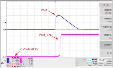
A colleague took a risk and touched the chip that failed to be programmed with his hand, and his fingers were burned and blistered. Using a multimeter to measure, it was found that the power pin and ground of the chip that failed to be programmed were short-circuited. The voltage of the programming power supply was normal. Therefore, based on experience, we speculated that it was very likely that the programming power supply had an abnormal high voltage output when the programmer was powered on, which broke down the target chip. Using an oscilloscope to capture the waveform of the programming power supply Vout at the moment the programmer was powered on confirmed our conjecture.
As shown in Figure 1, when the programmer is powered on, the programming power supply Vout has a pulse of up to 20.4V and a duration of 150ms output to the target chip. The target chip with a power supply of only 3.3V obviously cannot withstand such a high-voltage pulse.

Figure 1 Abnormal output of Vout at the moment of power-on
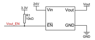
From the schematic diagram of the Vout power supply circuit in Figure 2, we can see that Vout is controlled by Vout_EN, and a low level enables Vout output. Vout_EN is pulled up to a high level of 3.3V, and Vout output should be disabled by default at the moment of power-on. How can there be this high-voltage pulse output?

Figure 2 Schematic diagram of Vout power supply circuit
From Figure 1, we can see that after Vout outputs 20.4V and lasts for nearly 30ms, Vout_EN is pulled up to a high level to disable Vout output, and then Vout gradually decreases to 0V. Why does Vout_EN take effect 30ms after Vout, instead of being effective as soon as power is turned on?
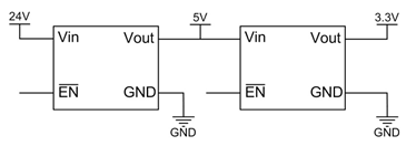
Let's look at Figure 3. 3.3V is converted from 24V to 5V and then converted again. Therefore, it takes a certain amount of time to generate 3.3V, and the corresponding Vout_EN also takes a certain amount of time to be effective. It is precisely because of this time difference that Vout can output a high-voltage pulse of 20.4V.

Figure 4 3.3V power supply schematic
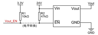
To solve the problem of enable signal lag, the best solution is to use the input power Vin as the enable level. When the input power is powered on, the output of Vout can be directly disabled. A level conversion circuit is added between Vout_EN and the Vin enable level, so that the 3.3V level Vout_EN can normally control the output of Vout after the program is running. After the improvement, the high-voltage pulse at the moment of power-on is perfectly eliminated.

Figure 5 Improved Vout power supply circuit
Therefore, in the process of product design, there can be no negligence and only with ingenuity can we create high-quality products.
Previous article:Brief Analysis of Preliminary Testing of Photovoltaic Inverters
Next article:How to avoid static electricity damage to laboratory equipment
- Popular Resources
- Popular amplifiers
- "Cross-chip" quantum entanglement helps build more powerful quantum computing capabilities
- Why is the vehicle operating system (Vehicle OS) becoming more and more important?
- Car Sensors - A detailed explanation of LiDAR
- Simple differences between automotive (ultrasonic, millimeter wave, laser) radars
- Comprehensive knowledge about automobile circuits
- Introduction of domestic automotive-grade bipolar latch Hall chip CHA44X
- Infineon Technologies and Magneti Marelli to Drive Regional Control Unit Innovation with AURIX™ TC4x MCU Family
- Power of E-band millimeter-wave radar
- Hardware design of power supply system for automobile controller
 Professor at Beihang University, dedicated to promoting microcontrollers and embedded systems for over 20 years.
- Intel promotes AI with multi-dimensional efforts in technology, application, and ecology
- ChinaJoy Qualcomm Snapdragon Theme Pavilion takes you to experience the new changes in digital entertainment in the 5G era
- Infineon's latest generation IGBT technology platform enables precise control of speed and position
- Two test methods for LED lighting life
- Don't Let Lightning Induced Surges Scare You
- Application of brushless motor controller ML4425/4426
- Easy identification of LED power supply quality
- World's first integrated photovoltaic solar system completed in Israel
- Sliding window mean filter for avr microcontroller AD conversion
- What does call mean in the detailed explanation of ABB robot programming instructions?
- STMicroelectronics discloses its 2027-2028 financial model and path to achieve its 2030 goals
- 2024 China Automotive Charging and Battery Swapping Ecosystem Conference held in Taiyuan
- State-owned enterprises team up to invest in solid-state battery giant
- The evolution of electronic and electrical architecture is accelerating
- The first! National Automotive Chip Quality Inspection Center established
- BYD releases self-developed automotive chip using 4nm process, with a running score of up to 1.15 million
- GEODNET launches GEO-PULSE, a car GPS navigation device
- Should Chinese car companies develop their own high-computing chips?
- Infineon and Siemens combine embedded automotive software platform with microcontrollers to provide the necessary functions for next-generation SDVs
- Continental launches invisible biometric sensor display to monitor passengers' vital signs
- How to use the ratiometric characteristics of sensors and ADCs to improve accuracy
- Read and write SD card in Uboot with SIN-IMX6UL development board
- P89LPC932 Chinese Device Manual
- ARM multiplication instructions and multiply-add instructions
- Is it possible to estimate the gain of an antenna in this way?
- How to display text in different fonts in an edit control
- Supercapacitors: Materials, Systems and Applications
- Skills required by MCU engineers and embedded engineers
- Three types of NAND Flash applications
- MSP430 clock system problem

 TLC2654AM-8DR


 京公网安备 11010802033920号