The digitization of all media, including audio, video, and images, has put forward higher and higher requirements for signal processing. These digital signal data contents need to be created, stored, transmitted, and replayed. At the same time, more and more communication and entertainment transmission systems are portable, which requires greatly improved signal processing bandwidth. The growing signal processing load makes electrical power consumption a limiting factor for signal processing systems.
DSP is an excellent choice for digital signal processing because digital signal processors can be programmed and can easily handle many changing standards in today's rapidly changing world of digital media processing. However, the "generality" of general-purpose DSPs makes it not very power-efficient for all applications.
Hard-wired signal processing modules usually have better power efficiency, but lack the flexibility and programmability of DSPs. Configurable processor technology builds a bridge between the flexibility and programmability of fixed ISA (instruction set architecture) of DSP and the power efficiency of hard-wired modules by building a DSP with the correct, feature-rich and programmable attributes for a specific task. Tensilica's Vectra LX is a good example of this concept. Vectra LX is a fixed-point vector DSP engine built on the basis of the Xtensa LX configurable processor through configuration options.
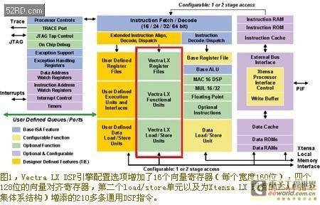
The Vectra LX fixed-point DSP engine is a configuration of the Xtensa LX microprocessor core. The fixed-point DSP engine is a 3-issue SIMD processor with four multipliers/accumulators (four MACs) that can process
128-bit vectors. The 128-bit vector can be divided into eight 16-bit or four 32-bit elements. The entire Vectra LX DSP engine is developed in the TIE (Tensilica's Instruction Extension) language and can be modified to suit the target application area. As shown in Figure 1, the Vectra LX DSP engine adds 16 vector registers (each 160 bits wide), four 128-bit vector queue registers, a second load/store unit, and more than 210 common DSP instructions in the existing Xtensa LX processor instruction set architecture.
The basic Xtensa LX processor is a single-issue microprocessor with 16-bit and 24-bit instructions. However, Tensilica's processor generator enables developers to add wider instruction word lengths. Multiple independent operations are added to the processor instruction set through a technology called FLIX (Flexible-Length Instruction Extensions). FLIX instructions can be 32-bit or 64-bit wide, and because the Xtensa LX processor has been designed to handle multiple instruction widths, multi-operation FLIX instructions can be freely combined in the processor code flow and can be linked together with existing single-issue Xtensa LX processor instructions.
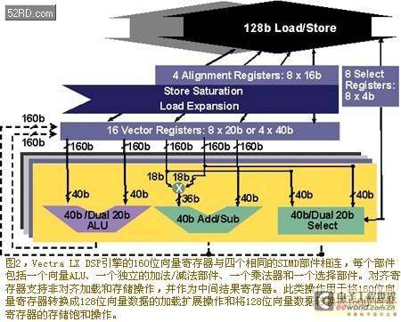
When developers select the Vectra LX DSP engine configuration option, Tensilica's processor generator automatically adds the RTL code for the DSP engine to the synthesizable Xtensa LX processor. The new Vectra LX instructions are added to the software toolset (compiler, assembler, debugger, instruction set simulator ISS and real-time operating system RTOS interface) that is automatically generated by the processor. Vectra LX increases the gate count of the Xtensa LX processor by 200,000 to 250,000 gates. Most of these additional gates are used to build the registers and execution components in the Vectra LX DSP engine. Because the general processor and DSP engine extension can share the existing instruction fetch and instruction decoding components in the processor, those hardware modules do not need to be replicated. However, some logic needs to be added to decode the new instructions. Figure 2 is a block diagram of the registers and execution components added in the Vectra LX DSP engine configuration options.

Figure 3 shows the three-operation Vectra LX instruction word format. The rightmost four bits in the instruction word indicate that the instruction is 64 bits wide. The remaining 60 bits of the instruction word are distributed in three operation instruction slots of unequal length: one 24-bit and two 18-bit instruction slots. The 24-bit operation instruction slot in the Vectra LX instruction word (bits 4 to 27 in the instruction word) can hold all 80 basic instructions in the Xtensa LX processor, including the operation that controls the first load/store unit. This operation instruction slot can also handle extended 128-bit load/store instructions, which can store information into the Vectra LX wide vector register and can also read information from the vector register.
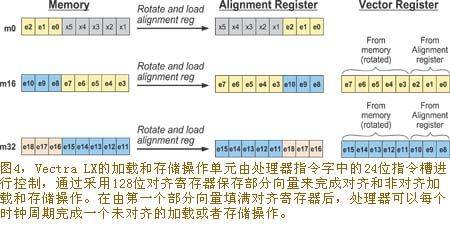
The 24-bit operation instruction slot can provide a wide enough encoding bit number to allow load and store instructions to specify aligned or unaligned load and store operations in the instruction slot, as shown in Figure 4. Unaligned load and store operations help related vectorization compilers to handle memory data arrays that can be aligned in any way, because the code generated by the compiler is sometimes unaligned data arrays, which will reduce the performance of the DSP. However, this performance loss can be compensated by the support provided by the DSP engine in the form of unaligned load and store operations.
The Vectra LX DSP engine's aligned registers provide partial vector storage capabilities. These aligned registers are initialized with the first partial vector at the beginning of an unaligned load or store string. Subsequent unaligned load or store operations implicitly merge with the new vector data, which is rotated and concatenated with the contents of the partial aligned registers to group the entire vector together in the aligned registers. These unaligned load and store operations also prepare the aligned registers for the next unaligned load or store operation, so that a series of consecutive unaligned load or store operations can move data into or out of the unaligned data array with approximately the same efficiency as aligned data. The
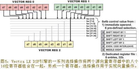
Vectra LX DSP engine uses the first 18-bit operation instruction slot (bits 28 to 45) to place 4×40-bit SIMD single instruction multiple data multiply-accumulate MAC operations. This instruction slot also performs the DSP engine's select operation, which can group eight 16-bit registers from two source vector registers together, as shown in Figure 5. The
Vectra LX processor select operation can be used to implement vector operations such as copy, rotate, shift, and data interleaving. The second 18-bit operation instruction slot (bits 46 to 63) stores the DSP engine's 4×40-bit and 8×20-bit SIMD single-instruction multiple-data ALU operations and those used to control the second load/store unit in the processor, which can perform data alignment operations and 128-bit vector load and store operations.
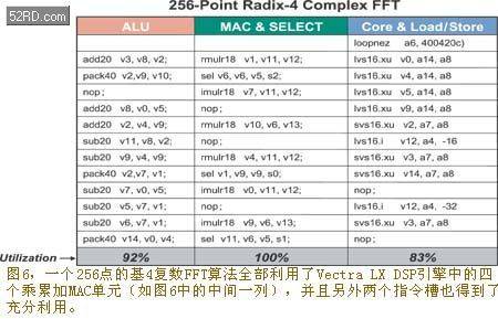
The Xtensa LX and Vectra LX processors efficiently execute DSP code using three instruction slots. Figure 6 shows a compact loop for a 256-point radix-4 complex FFT algorithm. All four multiply-accumulate MAC units are fully utilized (as shown in the middle column of Figure 6), and the other two instruction slots are also fully utilized. As a result of organizing the program in this way, the Vectra LX DSP engine greatly reduces the number of clock cycles required to perform DSP tasks using the Xtensa LX processor. Figure 7 shows the clock cycle count for the 256-point radix-4 FFT algorithm.
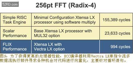
A basic Xtensa LX processor configuration requires 155,000 clock cycles to calculate a 256-point radix-4 complex FFT algorithm. If a 32-bit multiplier is added to the basic processor configuration, the same FFT algorithm requires 23,633 clock cycles, which is nearly an order of magnitude less; if SIMD and multi-operation capabilities are added as in the Vectra LX DSP engine, it requires 944 clock cycles, which is more than two orders of magnitude less, and the performance is improved by about 156 times.
Software Environment
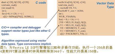
Exploiting DSP architecture performance requires software tools to understand and effectively use the architectural features of the DSP. A vectorized C/C++ compiler called XCC supports the Xtensa LX and Vectra LX architectures. The compiler automatically handles vector data types in the same way as traditional C data types, as shown in Figure 8. Conversions to vector types are implicit.

To achieve higher processor performance, the XCC compiler seeks opportunities to vectorize the code using the Vectra LX SIMD execution unit, primarily targeting loop statements, as shown in Figure 9. When compiling the DSP code, the XCC compiler generates a continuous string of Vectra LX operations, which are then scheduled and packaged into Vectra LX wide instruction words, as shown in Figure 10. The scheduled assembler does the same for the assembly code.
The performance of the application proves that it is worthwhile to adopt a new architecture for the processor or DSP. You can see from the BDTIsimMark2000 typical program score that the FLIX language makes the Xtensa LX processor computing performance improve.

Figure 11 shows the BDTIsimMark2000 scores of the Xtensa LX and Vectra LX processors, and compares them with two other very fast DSP cores, the CEVA-X1620 and StarCore SC1400. The BDTIsimMark2000 scores are based on simulation results. During the test, the Xtensa LX and Vectra LX processors were simulated at a clock speed of 370 MHz, which can be implemented in a 130nm IC process using standard synthesis and place-and-route tools.
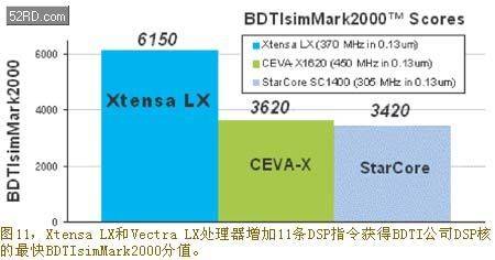
It is worth noting that the typical program scores for the Xtensa LX and Vectra LX processors are not simply obtained by adding the Vectra LX DSP engine to the Xtensa LX. Instead, 11 user-defined extension instructions are added using the TIE language, and the performance of the processor in executing typical programs is further improved through BDTI. Since the Xtensa LX is configurable, the expansion of the BDTI typical program directly reflects the use of the configurable Xtensa LX processor in actual applications.
In fact, the entire Vectra LX DSP engine is developed in the TIE language, and the SOC developer can modify it to suit the target application. An important reason for using a configurable processor is to maximize the processor's capabilities for the target application. In this case, the BDTI typical program is the target application, but the target application can also be audio, video, image or other types of signal processing.
Previous article:A brief analysis of the basic structure of DSP chips
Next article:Selection strategy of ASIC, FPGA and DSP in software radio design
Recommended ReadingLatest update time:2024-11-24 00:23


- Popular Resources
- Popular amplifiers
- "Cross-chip" quantum entanglement helps build more powerful quantum computing capabilities
- Why is the vehicle operating system (Vehicle OS) becoming more and more important?
- Car Sensors - A detailed explanation of LiDAR
- Simple differences between automotive (ultrasonic, millimeter wave, laser) radars
- Comprehensive knowledge about automobile circuits
- Introduction of domestic automotive-grade bipolar latch Hall chip CHA44X
- Infineon Technologies and Magneti Marelli to Drive Regional Control Unit Innovation with AURIX™ TC4x MCU Family
- Power of E-band millimeter-wave radar
- Hardware design of power supply system for automobile controller
 Professor at Beihang University, dedicated to promoting microcontrollers and embedded systems for over 20 years.
- STMicroelectronics discloses its 2027-2028 financial model and path to achieve its 2030 goals
- 2024 China Automotive Charging and Battery Swapping Ecosystem Conference held in Taiyuan
- State-owned enterprises team up to invest in solid-state battery giant
- The evolution of electronic and electrical architecture is accelerating
- The first! National Automotive Chip Quality Inspection Center established
- BYD releases self-developed automotive chip using 4nm process, with a running score of up to 1.15 million
- GEODNET launches GEO-PULSE, a car GPS navigation device
- Should Chinese car companies develop their own high-computing chips?
- Infineon and Siemens combine embedded automotive software platform with microcontrollers to provide the necessary functions for next-generation SDVs
- Continental launches invisible biometric sensor display to monitor passengers' vital signs
- Does Cadence have any built-in package?
- Introduction to Commonly Used Resistors
- Please explain the principle of this boost circuit
- Disassembling Children's LED Electronic Watch
- Find a book specifically about C++ move semantics
- DSP SCI serial port problem
- Career Options
- Hybrid Electric Vehicle (HEV) Main Technology Assembly
- ST BlueNRG-LP Evaluation Board DesignSpark Unboxing
- TI Engineer's Annual Review: Processors (Hot Products: MSP430, C2000, C6000 Multicore, etc.) Selected Q&A

 MATLAB and FPGA implementation of wireless communication


 京公网安备 11010802033920号