Abstract: One of the key technologies of digital camera night visibility instrument is to process the image information of target light source and black body collected by CCD at high speed and in real time. A miniaturized and portable embedded visibility measurement system based on TMS320DM642 is designed, implemented in hardware and software, and applied to the night visibility measurement of digital camera. The PAL video stream of 25 frames/s is collected by CCD, digitized and sent to DSP processor, and the image segmentation and positioning algorithm of target light source and black body is realized by DSP to complete the measurement of digital camera night visibility. The experimental results show that the designed embedded system can well complete the night visibility measurement.
Keywords: DSP; image processing; night visibility; embedded system
0 Introduction
Visibility is an important parameter in meteorological observation, and it has important application value in aviation, railways, highways, etc. Digital camera method is a relatively new method of detecting visibility, which automatically obtains visibility value based on the definition of visibility and the visual threshold effect of human eyes. Its basic idea is to directly process the image of the selected target object captured by the camera (CCD) and analyze the brightness information to obtain the visibility value. This article studies the night visibility measurement method of dual light source camera method, designs a miniaturized embedded system based on DSP, and designs a method for measuring night visibility from both hardware and software design aspects.
The system is studied and the calculation of night visibility is realized. The experimental results show that the system can be used for observing night visibility.
1 Principle of digital camera detection of night visibility
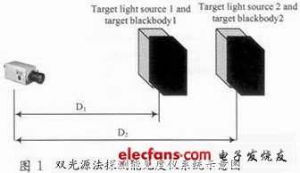
The principle of using the dual light source method to carry out nighttime visibility detection is shown in Figure 1.

The dual light source method is based on the Beer-Lambert law. It uses the image grayscale information to obtain the brightness attenuation of the light source and the black body, and then inverts the atmospheric extinction coefficient to calculate visibility. The atmospheric extinction coefficient is:![]()
Where: are the apparent brightness of light sources 1, 2, and black bodies 1, 2 respectively; D1 and D2 are the distances from light sources 1, 2 to the camera respectively.
According to the visual threshold effect of the human eye, the visibility value is D=ln(1/0.02)/σ.
2 Embedded System Hardware Design
2.1 Overall system design
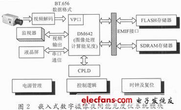
The system is mainly composed of a target light source and black body, a camera and a signal processing platform. The signal processing platform completes the image acquisition, segmentation and visibility calculation functions of the signal. This paper designs a real-time image acquisition and processing platform with TMS320DM642 as the core, combined with CY37064P100, TVP5150PBS, SAA7121, and DMT32240T035_01WN. The platform completes the image acquisition and segmentation and positioning processing, and calculates the brightness and visibility value of the target light source and target black body. Figure 2 is a system module structure diagram.

The PAL camera provides a video stream of 25 frames/s. The CCD captures images and converts the input video stream into 8-bit ITU-R BT.656 format video data through the video decoding chip, and obtains the visibility value through DSP image processing. Then, the DM642 extended serial communication circuit communicates with the LCD screen with a serial port, and the visibility value is displayed on the LCD screen. At the same time, the video encoding chip converts the BT.656 format video data processed by the DSP into a PAL format video signal, and displays the processed target light source and target black body images through the monitor.
2.2 Embedded Signal Processing System Hardware Design
2.2.1 Video Capture Module
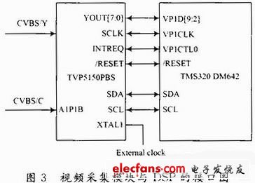
An 8-bit analog industrial camera is used to directly capture PAL video images and send them to the video decoder. After decoding, the data is output in ITU-R BT.656 format. The decoder uses the high-performance, small package (32-pin TQFP), low power consumption (less than 150 mW) TVP5150PBS to convert the PAL video signal into a digital color difference signal (YUV 4:2:2). Figure 3 is a diagram of the interface between the video decoding module and the DSP.

A voltage divider resistor network is designed between the external video input (0~1 Vpp) and the TVP5150PBS video input to make the input level of the TVP5150PBS 0~0.75 Vpp.
The system sets the A channel of the video port VP1 as the video input port. The I2C interface of TMS320DM642 realizes the initialization and configuration of the internal registers of the TVP5150 chip. The SCL and SDA pins of the TVP5150 chip are respectively connected to the clock and data address lines of the TMS320DM642. The timing of SCL and SDA is used to complete the writing and reading of data from the DSP to the video decoder chip register. TVP5150 receives the video information of the camera and outputs the decoded data serially. The digital video stream contains the odd and even field indicator signal FI, field synchronization signal, line synchronization signal, pixel clock, YUV data output and other elements, and the data rate is about 165 Mb/s.
2.2.2 Image Processing Module
The system uses TI's 32-bit fixed-point DSP chip TMS320DM642 for digital media applications to complete the signal processing process. The BT.656 video stream output by TVP5150 is stored in the 2 560 B VP1A channel FIFO after passing through the video port of TMS320DM 642. Due to the large amount of image data, an external off-chip memory is required to store image data information. The data in the FIFO is moved to the off-chip memory SDRAM through the EDMA channel. When the A channel of the video port VP1 has a video Y, U, V component data transfer request, the EDMA processing function will be triggered in the program to complete the transfer of FIFO data to SDRAM. VP1EVTYA, VP1EVTUA, and VP1EVTVA are events related to the video Y, U, and V components that occur on the VP1A channel, respectively, and are connected to the corresponding channels of DM642 EDMA. After the FIFO transfers data to SDRAM, the program running in FLASH starts to call the image data, perform algorithm processing, obtain the brightness values of the light source and the black body, and complete the visibility calculation.
2.2.3 Video display module
The video display part converts the BT.656 format video data into a PAL format video signal through the video encoding chip, and then sends it to the monitor to display the processed target light source and target black body image. The SAA7121H encoder is used to set the VP0 A channel of the TMS320DM642 as the video output port. Figure 4 is a connection diagram between the video encoding module and the DSP, and CVBS_OUT is the composite video output by decoding. Like the TVP5150, the configuration of each register inside the SAA7121 chip is configured through the I2C interface of the TMS320DM642, and the I2C bus of the TMS320DM642 can be shared with the TVP5150.

2.2.4 Serial communication module
The system uses CY37064P100 and TL16C752B to expand the serial communication circuit outside the DSP to achieve communication between the main chip and the LCD screen with a serial port, and displays the night visibility value on the LCD screen. Figure 5 is the design diagram of the serial communication module. The serial port LCD screen is selected to display the visibility value and draw the historical curve.

3 Embedded System Software Design
3.1 System software design based on DSP/BIOS and RF5
DSP/BIOS is an embedded operating system based on CCS. Its multi-threading mechanism can facilitate the writing of multi-tasking applications. Compared with traditional DSP programs written in assembly language and C language, DSP/BIOS can effectively improve the efficiency of code execution and facilitate real-time monitoring of code execution. RF5 is an application design framework based on DSP/BIOS, which implements storage management, thread model and channel encapsulation. Using the RF5 reference framework can greatly reduce the difficulty and time of developers. According to system requirements, embedded software is written based on the RF5 reference framework. Figure 6 is a software program flow chart.

Each processing task uses the SCOM message mechanism to communicate with each other. After the image acquisition task collects data, it transmits it to the processing task through the SCOM message; after the processing task performs relevant processing and visibility calculation on the image, it notifies the acquisition task to perform the next acquisition processing, and transmits the processing results to the output task for display. At the same time, the processing task coordinates the communication between this task and the other two tasks.
3.2 Research on image processing algorithms for visibility calculation
The visibility calculation task is the core of DSP embedded software, and its image processing method is the key to system reliability. The digital camera night visibility instrument calculates the brightness of the target light source after two light sources of the same brightness have been attenuated at different distances through image processing, and completes the measurement of visibility value by inverting the atmospheric extinction coefficient based on the brightness. Its image processing process is mainly divided into three parts: image preprocessing, image segmentation and positioning, and calculation of visibility value.
3.2.1 Image Preprocessing
Image preprocessing mainly involves image filtering of the collected light source image to remove the influence of background noise and stray light, so as to make the brightness of the target light source and black body image uniform. Since the visibility meter of this system is mainly installed on highways for visibility warning, the image clarity is not high under weather conditions such as low fog and rainy days. In addition, CCD will also generate corresponding noise pollution during the process of image acquisition and transmission. Therefore, it is necessary to preprocess the image.
The frequency domain enhancement method is used to make the image clear. The image is Fourier transformed, filtered in the frequency domain, and then the filtered image is inversely transformed to the spatial domain to obtain an enhanced image. In addition, the wavelet threshold denoising method is used to utilize the good effect of wavelet transform in the field of signal denoising and data compression. Based on the different frequencies and amplitudes of signals and noise, the image is subjected to a two-dimensional wavelet transform. According to the difference between the original information of the image and the wavelet transform coefficients of the noise, a threshold is set to remove the noise elements in the wavelet coefficients. The processed wavelet coefficients are used to perform a two-dimensional wavelet inverse transform to obtain the denoised image.
3.2.2 Image segmentation and positioning
The key to measuring nighttime visibility with digital camera is to accurately extract the brightness information of the image. In the process of brightness calculation, accurately segmenting the light source image is the key to the calculation process. Simple threshold segmentation is prone to misjudgment and affects the calculation of visibility. Image segmentation studies the segmentation algorithm suitable for two target light sources and black bodies, and takes the part of the light source with relatively uniform brightness as the brightness value of the light source and the black body.
Select a suitable USAN area and use the SUSAN edge detection operator to perform edge detection on the image. Segment the image based on the obtained edge to obtain a binary image of the light source. Take a square template to search and calculate the brightness value in the light source part, and find the area with the highest brightness in the box, and use this area as the brightness value of the light source. Then, based on the relationship between the image size and the corresponding number of pixels, find the position of the black body and calculate the black body brightness value. Figure 7 shows the process from image segmentation to positioning.

3.2.3 Calculation of visibility values
Usually, the real-time requirements for visibility changes are not high. According to the efficiency of DSP calculation, 100 pictures can be superimposed to calculate the average brightness, and then the calculated brightness values of the target light source and target black body are substituted into the extinction coefficient σ and visibility D calculation formula respectively to complete the visibility calculation.
4 Experimental effect analysis
The Dongpu Island observation site in Hefei was selected for the visibility experiment. In the experiment, 100 frames of images were averaged to obtain the brightness value. Figure 8 shows the display of the visibility value calculated by the embedded system through the serial port LCD screen.

According to the weather conditions in Hefei in June, the experiment took the night from 19:30 to 5:00 the next day as the night to measure visibility. Figure 9 shows the measurement results from June 8 to June 12, 2012. From the measurement results, it can be seen that the digital camera night visibility meter has almost the same change trend as the forward scattering visibility meter, and the maximum relative standard error is 15%, which meets the World Meteorological Organization's regulations that the standard visibility meter error is less than 20%.

5 Conclusion
The design scheme of the digital image processing platform based on DSP and CPLD designed in this paper can be applied to the nighttime visibility measurement of digital cameras to obtain real-time display of images and calculation of visibility. The image segmentation and positioning algorithm used can obtain a smaller brightness error, and the visibility value is also very close to the manual observation value, with an error within an acceptable 20%. The system has the characteristics of high reliability, strong real-time performance, and high speed. It has been verified by experiments that it meets the requirements of nighttime visibility measurement of digital cameras. In theory, it can be applied to the observation of nighttime visibility, and can be used as a platform for later research and development to continue to carry out nighttime and daytime visibility detection of digital cameras.
Previous article:PCB through-hole rework tips: How to solder delicate PCB boards
Next article:Audio technology: Disintegration and MEMS microphones are the trend
Recommended ReadingLatest update time:2024-11-23 18:45


- Popular Resources
- Popular amplifiers
- USB Type-C® and USB Power Delivery: Designed for extended power range and battery-powered systems
- ROHM develops the second generation of MUS-IC™ series audio DAC chips suitable for high-resolution audio playback
- ADALM2000 Experiment: Transformer-Coupled Amplifier
- High signal-to-noise ratio MEMS microphone drives artificial intelligence interaction
- Advantages of using a differential-to-single-ended RF amplifier in a transmit signal chain design
- ON Semiconductor CEO Appears at Munich Electronica Show and Launches Treo Platform
- ON Semiconductor Launches Industry-Leading Analog and Mixed-Signal Platform
- Analog Devices ADAQ7767-1 μModule DAQ Solution for Rapid Development of Precision Data Acquisition Systems Now Available at Mouser
- Domestic high-precision, high-speed ADC chips are on the rise
- Intel promotes AI with multi-dimensional efforts in technology, application, and ecology
- ChinaJoy Qualcomm Snapdragon Theme Pavilion takes you to experience the new changes in digital entertainment in the 5G era
- Infineon's latest generation IGBT technology platform enables precise control of speed and position
- Two test methods for LED lighting life
- Don't Let Lightning Induced Surges Scare You
- Application of brushless motor controller ML4425/4426
- Easy identification of LED power supply quality
- World's first integrated photovoltaic solar system completed in Israel
- Sliding window mean filter for avr microcontroller AD conversion
- What does call mean in the detailed explanation of ABB robot programming instructions?
- STMicroelectronics discloses its 2027-2028 financial model and path to achieve its 2030 goals
- 2024 China Automotive Charging and Battery Swapping Ecosystem Conference held in Taiyuan
- State-owned enterprises team up to invest in solid-state battery giant
- The evolution of electronic and electrical architecture is accelerating
- The first! National Automotive Chip Quality Inspection Center established
- BYD releases self-developed automotive chip using 4nm process, with a running score of up to 1.15 million
- GEODNET launches GEO-PULSE, a car GPS navigation device
- Should Chinese car companies develop their own high-computing chips?
- Infineon and Siemens combine embedded automotive software platform with microcontrollers to provide the necessary functions for next-generation SDVs
- Continental launches invisible biometric sensor display to monitor passengers' vital signs
- MSP430 timer output PWM waveform example
- 【AD21】The mouse cannot be moved to the left and bottom of the PCB origin. What is the solution?
- 2021 ON Semiconductor Avnet RSL10 Bluetooth SoC Development and Design Competition Second Post (Initial Modification Routine)
- Improving efficiency is a universal requirement for power supplies and electronic transformers
- CC2531 Zlight2 Reference Design
- Fundamentals of Electronic Design (Huang Genchun)
- MSP430g2553 hardware UART (modification based on official routines)
- [TI recommended course] #Innovation of general-purpose op amp and comparator chips#
- Recently, I am doing an experiment on communication between DSP and AD5390. DSP controls AD5390 through SPI bus. I am not familiar with the core of AD5390.
- A new year and a new beginning. I wish you all a happy New Year!

 MATLAB and FPGA implementation of wireless communication


 京公网安备 11010802033920号