|
The OP
Published on 2020-9-4 11:55
Only look at the author
This post is from ARM Technology
| |||||||||||||||||||||||||||||||||||||||||||||||||||||||||||||||||||||||||||
|
|
|||||||||||||||||||||||||||||||||||||||||||||||||||||||||||||||||||||||||||
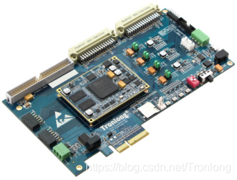
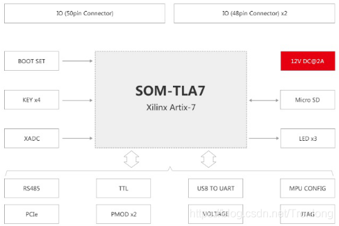
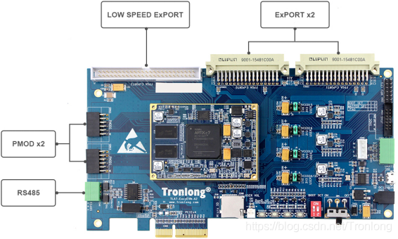
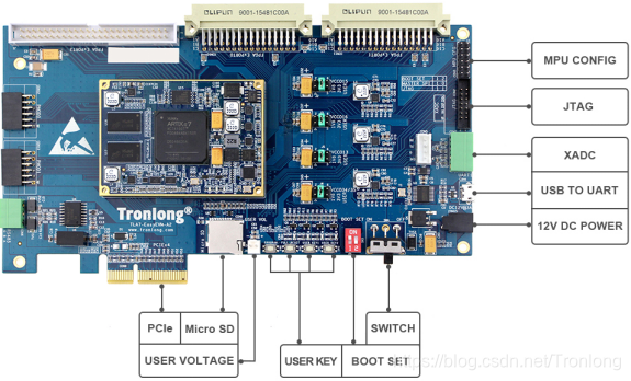
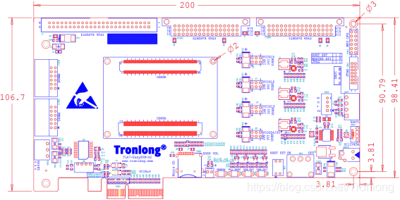
- 【Posts】TLA7-EasyEVM is a development board based on Xilinx Artix-7 series FPGA processor
- 【Posts】Xilinx Zynq-7015 SoC Industrial Core Board SOM-XQ7Z15 Cortex-A9 + Artix-7
- 【Posts】[Xilinx FPGA domestic replacement] ANLOGIC replaces Xilinx Spartan series
- 【Posts】High-efficiency integrated power supplies from Texas Instruments for NXP processors and Xilinx FPGAs
- 【Posts】Xilinx FPGA application advanced general IP core detailed explanation and design development
- 【Posts】[Evaluation of domestic FPGA Gaoyun GW1N series development board]——(5) Design of the programmer
- 【Posts】[Evaluation of domestic FPGA Gaoyun GW1N-4 series development board]——4. Use of embedded logic analyzer
- 【Posts】Regarding FPGA development, compared with several major companies' EDA design tools, Xilinx's Vivado is still the best
- 【Download】WP373-Xilinx launches three new series of FPGAs: Virtex-7, Kintex-7, and Artix-7
- 【Download】Xilinx Artix-7 FPGA Data Sheet: DC and Switching Characteristics
- 【Download】Xilinx 7 Series FPGA LVDS Interface Application
- 【Download】Xilinx7 series FPGA entry-level image processing V1
- 【Download】Detailed Explanation of Xilinx Series FPGA Chip IP Cores [Edited by Liu Donghua]
- 【Download】16-layer official Xilinx Kintex UltraScale FPGA KCU105+4 DDR4.rar
- 【Download】FPGA Development Board Red Hurricane II Generation-Xilinx Edition Schematic Diagram (PDF)
- 【Download】Genesys Virtex-5 Xilinx FPGA Development Board Schematics and Documentation
- 【Design】NiteFury: A development board based on Artix-7 FPGA with DDR3 RAM for developing PCIe, etc.
- 【Design】Powering Xilinx Zynq 7000 Series SoC/FPGA Evaluation Module with Single Power Management IC
- 【Design】MAXREFDES1126: 0.72V/20A power supply for Xilinx Ultrascale+ FPGAs
- 【Design】MAXREFDES1131: 0.72V/12A power supply for Xilinx Ultrascale+ FPGA
- 【Design】Xilinx FPGA minimum system schematic diagram (XC3S400+USB2 practical)
- 【Design】Novena: an open source computer based on Freescale and Xilinx FPGA, designed for use as a desktop, laptop or standalone board
- 【Articles】Mir FPGA core board is on the market! Domestic Unisplendour Logos-2 core board and Xilinx Artix-7 core board
- 【Articles】Xilinx Kintex-7 FPGA DDR3 Interface Performance Demonstration
- 【Articles】Xilinx FPGA DIY Series (2): Digital Storage Sweeper
- 【Articles】Xilinx FPGA DIY Series (5): Implementation of an IF Fully Digital Spectrum Analyzer
- 【Articles】Configuration circuit of Xilinx Spartan-3 series FPGA
- 【Articles】Fast Startup for Xilinx FPGA
-
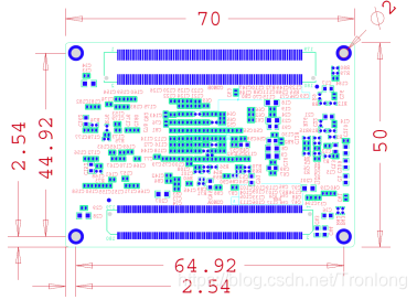
Xilinx Zynq-7015 SoC Industrial Core Board SOM-XQ7Z15 Cortex-A9 + Artix-7
Zynq-7015SoCIndustrialCoreBoard(SOM-XQ7Z15)1.IntroductiontothecoreboardSOM-XQ7Z15isaheterogeneousmulti-coreindustrialcoreboarddesignedbasedontheXilinxZynq-7000seriesXC7Z015high-performanceandlow-powerprocessorlaunchedbyGuangzhouXingqianElec ...
-
High-efficiency integrated power supplies from Texas Instruments for NXP processors and Xilinx FPGAs
TI'sbroadportfolioofpowermanagementICssupportstheneedsofNXPprocessorsandXilinxFPGAsBasedonuser-programmablePMICssuchastheTPS6521815,thesereferencedesignsenableuserstoprogramnonvolatileEEPROMmemorytogeneratedesiredvoltages,sequencing,andothe ...
-
[Follow me Season 2 Episode 4] Advanced Task 2: IMU machine learning to identify motion status
Tobehonest,althoughthemachinelearningcanrun,Ireallydon’tunderstandwhatthismachinelearninghastodowithitThemachinelearningtrainingisnotreflectedatall.materialUsingtheIMUMachineLearningCoreFeatures|ArduinoDocumentationLSM6DSOX/srcatmain·stm3 ...
- 【Follow me Season 2 Episode 4】Advanced Task 1: Displaying MIC amplitude using LED color
- 【Follow me Season 2 Episode 4】Task 3: MIC recording and waveform display
- ESP32 internal structure diagram
- SDIO connection to TF card initialization failed
- Servo Motor
- This Wednesday's award-winning live broadcast: 5G conformance testing and device acceptance testing
- What should we pay attention to during the embedded learning process?
EEWorld Datasheet Technical Support
-
"Cross-chip" quantum entanglement helps build more powerful quantum computing capabilities
IBM scientists have achieved "cross-chip" quantum entanglement - successfully entangled two "Eagl
-
Ultrasound patch can continuously and noninvasively monitor blood pressure
A research team at the University of California, San Diego, has developed an innovative wearable
-
Europe's three largest chip giants re-examine their supply chains
At the Electronica 2024 CEO Roundtable held just last week, the CEOs of three chip giants, Infine
- It is reported that Kioxia will be approved for listing as early as tomorrow, and its market value is expected to reach 750 billion yen
- The US government finalizes a $1.5 billion CHIPS Act subsidy to GlobalFoundries to support the latter's expansion of production capacity in the US
- SK Hynix announces mass production of the world's highest 321-layer 1Tb TLC 4D NAND flash memory, plans to ship it in the first half of 2025
- UWB is a new way to use it in cars. Can wireless BMS also use it?
- Filling the domestic gap! China Mobile, Huawei and others jointly released the first GSE DPU chip
- Samsung Electronics NRD-K Semiconductor R&D Complex to import ASML High NA EUV lithography equipment
- Apple reveals the secret of its own chip success: competitors can't use the latest cutting-edge technology
- Problems with STM32 and passive buzzer playing sound
- Embedded Tutorial_DSP Technology_DSP Experiment Box Operation Tutorial: 2-28 Building a Lightweight WEB Server Experiment
- OPA847IDBVR op amp domestic replacement
- AG32VF407 Test UART
- [Digi-Key Follow Me Issue 2] Chapter 1: Sharing on receiving the goods
- What model is this infrared receiver? Which model can be used instead? Thank you
- Selling brand new unopened ZYNQ 7Z020 FPGA core board
- The LORA module used in the lithium battery-powered water meter setting can save energy when 100 water meters are installed in one corridor.
- I would like to ask, when a port is set to RX0, is it necessary to set the input and output direction of this port?
- Why is this year so difficult? It’s even more difficult than during the pandemic. I’m 30 and facing unemployment. I’m so confused.
- Ask about the voltage regulator test question
- [Xiaohua HC32F448 Review] About Xiaohua Semiconductor's UART interrupt sending and PRINTF construction and redirection
- 【BIGTREETECH PI development board】 HDMI output test
- 【BIGTREETECH PI development board】+08. Audio test (zmj)
- [Xiaohua HC32F448 Review] +RTC electronic clock
- 有奖直播报名| 高可靠性IGBT新选择 —— 安世半导体650V IGBT
- 【直播时间】12月19日(周四)下午15:00-16:30
【直播好礼】定制双肩商务包、30元京东卡、吸管玻璃杯
- 安世半导体直播报名中
- 直播主题:安世半导体理想二极管与负载开关,保障物联网应用的稳健高效运行
直播时间:12月17日(周二)下午14:00
报名就有机会获得:定制双肩商务包、30元京东卡、吸管玻璃杯
- PI 电源小课堂 | 无 DC-DC 变换实现多路高精度输出反激电源
- 时间:即日起-12月15日
看视频学习电源干货,答题赢取京东卡!
- 参会有好礼 | 2024 瑞萨电子MCU/MPU工业技术研讨会
- 深圳站:11月30日(周六)深圳湾万怡酒店
上海站:12月06日(周五)上海喜玛拉雅酒店
奖励设置:现金红包、螺丝刀套装或30元京东卡
- Littelfuse 新品赋能电子产品安全可靠并高效, 10+挑战等你探索!
- Littelfuse 应用赋能星球,覆盖了诸多应用痛点及解决办法,邀请工程师一起探索,解锁更多设计力!
- 下载资料赢好礼!看Vicor模块化电源解决方案如何推动创新
- 活动时间:即日起-2024年12月31日
如何参与:点击活动页内您想了解的模块,找到资料下载即可参与抽奖,活动结束后统一发奖!
- 有奖活动|英飞凌高密度双相电源模块为高性能运算平台而生
- 活动时间:即日起-12月15日
活动奖励:蓝牙音箱、氮化镓充电器套装、黑色小背包
- 本周精选下载推荐:电源管理基础Dummies
- 本周小编给大家带来一本超简单、超干货的电子书——《电源管理基础Dummies》!内容深入浅出,排版舒服简洁,分分钟能get到电源管理最核心的知识内容。
EEWorld
subscription
account

EEWorld
service
account

Automotive
development
circle

About Us Customer Service Contact Information Datasheet Sitemap LatestNews
- I want to get started with 51 single-chip microcomputer hardware, what should I do?
- I want to get started with AVR microcontroller C language development, what should I do?
- I want to get started with pytorch convolutional neural networks, what should I do?
- I want to get started with microcontroller simulation, what should I do?
- I want to get started with convolutional neural networks, what should I do?
- For PCB practice entry, please give a study outline
- Please give a learning outline for the basic introduction of neural network algorithms
- How to get started with convolutional neural networks
- What microcontrollers should I learn for beginners?
- Basic knowledge of analog electronics technology


 Room 1530, Zhongguancun MOOC Times Building,
Block B, 18 Zhongguancun Street, Haidian District,
Beijing 100190, China
Tel:(010)82350740
Postcode:100190
 京公网安备 11010802033920号


 提升卡
提升卡 变色卡
变色卡 千斤顶
千斤顶